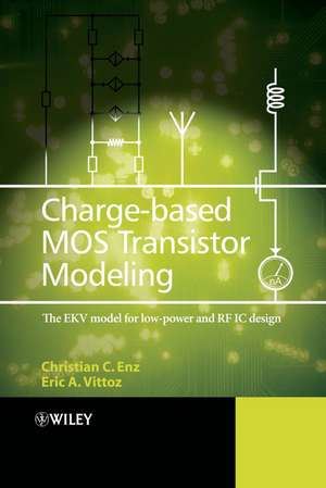
Charge–Based MOS Transistor Modeling – The EKV Model for Low–Power and RF IC Design
Autor C Enzen Limba Engleză Hardback – 13 iul 2006
Preț: 839.70 lei
Preț vechi: 922.74 lei
-9% Nou
Puncte Express: 1260
Preț estimativ în valută:
160.70€ • 167.15$ • 132.66£
160.70€ • 167.15$ • 132.66£
Carte tipărită la comandă
Livrare economică 15-29 aprilie
Preluare comenzi: 021 569.72.76
Specificații
ISBN-13: 9780470855416
ISBN-10: 047085541X
Pagini: 328
Dimensiuni: 170 x 244 x 19 mm
Greutate: 0.76 kg
Editura: Wiley
Locul publicării:Chichester, United Kingdom
ISBN-10: 047085541X
Pagini: 328
Dimensiuni: 170 x 244 x 19 mm
Greutate: 0.76 kg
Editura: Wiley
Locul publicării:Chichester, United Kingdom
Public țintă
- Designers, practicing engineers in the semiconductor device field and electronics systems industry.
- RF circuit designers and engineers
- Postgraduate students of electrical and computer engineering.
Cuprins
Foreword.
Preface.
List of Symbols.
1. Introduction.
1.1 The Importance of Device Modeling for IC Design.
1.2 A Short History of the EKV MOST Model.
1.3 The Book Structure.
PART I: THE BASIC LONG-CHANNELINTRINSIC CHARGE-BASED MODEL.
2. Introduction.
2.1 The N-channel Transistor Structure.
2.2 Definition of charges, current, potential and electric fields.
2.3 Transistor symbol and P-channel transistor.
3. The Basic Charge Model.
3.1 Poisson's Equation and Gradual Channel Approximation.
3.2 Surface potential as a Function of Gate Voltage.
3.3 Gate Capacitance.
3.4 Charge Sheet Approximation.
3.5 Density of Mobile Inverted Charge.
3.6 Charge-Potential Linearization.
4. Static Drain Current.
4.1 Drain Current Expression.
4.2 Forward and Reverse Current Components.
4.3 Modes of Operation.
4.4 Model of Drain Current Based on Charge Linearization.
4.5 Fundamental Property: Validity and Application.
4.6 Channel Length Modulation.
5. The Small-Signal Model.
5.1 The Static Small-Signal Model.
5.2 A General Non-Quasi-Static Small-Signal Model.
5.3 The Quasi-Static Dynamic Small-Signal Model.
6. The Noise Model.
6.1 Noise Calculation Methods.
6.2 Low-Frequency Channel Thermal Noise.
6.3 Flicker Noise.
6.4 Appendices.
Appendix : The Nyquist and Bode Theorems.
Appendix : General Noise Expression.
7. Temperature Effects and Matching.
7.1 Introduction.
7.2 Temperature Effects.
PART II: THE EXTENDED CHARGE-BASED MODEL.
8. Non-Ideal Effects Related to the Vertical Dimension.
8.1 Introduction.
8.2 Mobility Reduction Due to the Vertical Field.
8.3 Non-Uniform Vertical Doping.
8.4 Polysilicon Depletion.
8.4.1 Definition of the Effect.
8.5 Band Gap Widening.
8.6 Gate Leakage Current.
9. Short-Channel Effects.
9.1 Velocity Saturation.
9.2 Channel Length Modulation.
9.3 Drain Induced Barrier Lowering.
9.4 Short-Channel Thermal Noise Model.
10. The Extrinsic Model.
10.1 Extrinsic Part of the Device.
10.2 Access Resistances.
10.3 Overlap Regions.
10.4 Source and Drain Junctions.
10.5 Extrinsic Noise Sources.
PART III: THE HIGH-FREQUENCY MODEL.
11. Equivalent Circuit at RF.
11.1 RF MOS Transistor Structure and Layout.
11.2 What Changes at RF?.
11.3 Transistor Figures of Merit.
11.4 Equivalent Circuit at RF.
12. The Small-Signal Model at RF.
12.1 The Equivalent Small-Signal Circuit at RF.
12.2 Y-Parameters Analysis.
12.3 The Large-Signal Model at RF.
13. The Noise Model at RF.
13.1 The HF Noise Parameters.
13.2 The High-Frequency Thermal Noise Model.
13.3 HF Noise Parameters of a Common-Source Amplifier.
References.
Index.
Notă biografică
Christian C. Enz and Eric A. Vittoz are the authors of Charge-Based MOS Transistor Modeling: The EKV Model for Low-Power and RF IC Design, published by Wiley.
Descriere
As technology scales down to sub-micron dimensions the modelling of MOS device operation becomes of greater concern. The EKV model has been developed to facilitate the modelling and simulation of low voltage devices for application in low power semiconductor technologies.
