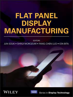
Flat Panel Display Manufacturing: Wiley Series in Display Technology
Autor J Souken Limba Engleză Hardback – 30 aug 2018
Din seria Wiley Series in Display Technology
- 24%
 Preț: 694.77 lei
 - 24%
 Preț: 691.97 lei
 - 9%
 Preț: 1287.71 lei
 - 9%
 Preț: 886.31 lei
 - 9%
 Preț: 1103.14 lei
 - 9%
 Preț: 778.46 lei
 - 9%
 Preț: 698.52 lei
 - 8%
 Preț: 681.04 lei
 - 9%
 Preț: 878.55 lei
 - 9%
 Preț: 729.76 lei
 - 8%
 Preț: 622.37 lei
 - 9%
 Preț: 793.56 lei
 - 9%
 Preț: 831.11 lei
 - 9%
 Preț: 778.96 lei
 - 9%
 Preț: 895.36 lei
 - 9%
 Preț: 980.23 lei
 - 9%
 Preț: 763.60 lei
 - 32%
 Preț: 750.38 lei
 - 32%
 Preț: 978.40 lei
 - 32%
 Preț: 694.68 lei
 - 31%
 Preț: 840.67 lei
 - 32%
 Preț: 538.13 lei
 - 30%
 Preț: 552.50 lei
 - 31%
 Preț: 536.22 lei
 - 30%
 Preț: 558.02 lei
Preț: 967.86 lei
Preț vechi: 1063.58 lei
-9% Nou
Puncte Express: 1452
Preț estimativ în valută:
185.22€ • 193.13$ • 153.94£
185.22€ • 193.13$ • 153.94£
Carte tipărită la comandă
Livrare economică 20 martie-03 aprilie
Preluare comenzi: 021 569.72.76
Specificații
ISBN-13: 9781119161349
ISBN-10: 1119161347
Pagini: 352
Dimensiuni: 203 x 254 x 27 mm
Greutate: 1.44 kg
Editura: Wiley
Seria Wiley Series in Display Technology
Locul publicării:Chichester, United Kingdom
ISBN-10: 1119161347
Pagini: 352
Dimensiuni: 203 x 254 x 27 mm
Greutate: 1.44 kg
Editura: Wiley
Seria Wiley Series in Display Technology
Locul publicării:Chichester, United Kingdom
Public țintă
Primary: Professionals and engineers in R&D departments for display–related technology developmentSecondary: Graduates and PhD students specialising in LCD/OLED/other flat panel displays
Cuprins
List of Contributors xxi Series Editor's Foreword xxv Preface xxvii 1 Introduction 1 Fang-Chen Luo, Jun Souk, Shinji Morozumi, and Ion Bita 1.1 Introduction 1 1.2 Historic Review of TFT-LCD Manufacturing Technology Progress 1 1.2.1 Early Stage TFT and TFT-Based Displays 2 1.2.2 The 1990s: Initiation of TFT-LCD Manufacturing and Incubation of TFT-LCD Products 2 1.2.3 Late 1990s: Booming of LCD Desktop Monitor and Wide Viewing Angle Technologies 4 1.2.4 The 2000s: A Golden Time for LCD-TV Manufacturing Technology Advances 4 1.3 Analyzing the Success Factors in LCD Manufacturing 5 1.3.1 Scaling the LCD Substrate Size 7 1.3.2 Major Milestones in TFT-LCD Manufacturing Technology 9 1.3.2.1 First Revolution: AKT Cluster PECVD Tool in 1993 9 1.3.2.2 Second Revolution: Wide Viewing Angle Technology in 1997 9 1.3.2.3 Third Revolution: LC Drop Filling Technology in 2003 10 1.3.3 Major Stepping Stones Leading to the Success of Active Matrix Displays 10 References 11 2 TFT Array Process Architecture and Manufacturing Process Flow 13 Chiwoo Kim 2.1 Introduction 13 2.2 Material Properties and TFT Characteristics of a-Si, LTPS, and Metal Oxide TFTs 15 2.2.1 a-Si TFT 15 2.2.2 LTPS TFT 16 2.2.2.1 Excimer Laser Annealing (ELA) 17 2.2.3 Amorphous Oxide Semiconductor TFTs 22 2.3 a-Si TFT Array Process Architecture and Process Flow 22 2.3.1 Four-Mask Count Process Architecture for TFT-LCDs 24 2.4 Poly-Si TFT Architecture and Fabrication 27 2.5 Oxide Semiconductor TFT Architecture and Fabrication 30 2.6 TFT LCD Applications 32 2.7 Development of SLS-Based System on Glass Display [1, 11, 14, 15] 33 References 35 3 Color Filter Architecture, Materials, and Process Flow 39 Young Seok Choi, Musun Kwak, and Youn Sung Na 3.1 Introduction 39 3.2 Structure and Role of the Color Filter 39 3.2.1 Red, Green, and Blue (RGB) Layer 40 3.2.1.1 Color Coordinate and Color Gamut 41 3.2.2 Black Matrix 44 3.2.3 Overcoat and Transparent Electrode 45 3.2.4 Column Spacer 46 3.3 Color Filter Manufacturing Process Flow 46 3.3.1 Unit Process 46 3.3.1.1 Formation of Black Matrix 46 3.3.1.2 Formation of RGB Layer 48 3.3.1.3 Overcoat (OC) 51 3.3.1.4 Formation of ITO Electrodes 53 3.3.1.5 Column Spacer (Pattern Spacer) 53 3.3.2 Process Flow for Different LC Mode 54 3.3.2.1 Color Filter for the TN Mode 54 3.3.2.2 Color Filter for the IPS Mode 54 3.3.2.3 Color Filter for the VA Mode 55 3.4 New Color Filter Design 55 3.4.1 White Color (Four Primary Colors) Technology 55 3.4.2 Color Filter on TFT 56 References 57 4 Liquid Crystal Cell Process 59 Heung-Shik Park and Ki-Chul Shin 4.1 Introduction 59 4.2 Liquid Crystal Cell Process 59 4.2.1 Alignment Layer Treatment 61 4.2.2 Process of Applying PI Layers 62 4.2.3 Rubbing Process 63 4.2.4 Photo-Alignment Process 64 4.2.5 LC Filling Process 65 4.2.5.1 Vacuum Filling Method 66 4.2.5.2 End Seal Process 66 4.2.5.3 One Drop Filling (ODF) Method 67 4.2.6 Vacuum Assembly Process 68 4.2.7 Polarizer Attachment Process 69 4.3 Conclusions 70 Acknowledgments 70 References 70 5 TFT-LCD Module and Package Process 73 Chun Chang Hung 5.1 Introduction 73 5.2 Driver IC Bonding: TAB and COG 73 5.3 Introduction to Large-Panel JI Process 74 5.3.1 COF Bonding 75 5.3.1.1 Edge Clean 75 5.3.1.2 ACF Attachment 76 5.3.1.3 COF Pre-Bonding 77 5.3.1.4 COF Main Bonding 78 5.3.1.5 Lead Check 78 5.3.1.6 Silicone Dispensing 78 5.3.2 PCB Bonding 79 5.3.3 PCB Test 79 5.3.4 Press Heads: Long Bar or Short Bar 79 5.4 Introduction to Small-Panel JI Process 79 5.4.1 Beveling 80 5.4.2 Panel Cleaning 80 5.4.3 Polarizer Attachment 80 5.4.4 Chip on Glass (COG) Bonding 81 5.4.5 FPC on Glass (FOG) Bonding 81 5.4.6 Optical Microscope (OM) Inspection 81 5.4.7 UV Glue Dispense 82 5.4.8 Post Bonding Inspection (PBI) 82 5.4.9 Protection Glue Dispensing 82 5.5 LCD Module Assembly 83 5.6 Aging 84 5.7 Module in Backlight or Backlight in Module 85 References 86 6 LCD Backlights 87 Insun Hwang and Jae-Hyeon Ko 6.1 Introduction 87 6.2 LED Sources 90 6.2.1 GaN Epi-Wafer on Sapphire 92 6.2.2 LED Chip 93 6.2.3 Light Extraction 94 6.2.4 LED Package 96 6.2.5 SMT on FPCB 97 6.3 Light Guide Plate 98 6.3.1 Optical Principles of LGP 98 6.3.2 Optical Pattern Design 99 6.3.3 Manufacturing of LGP 101 6.3.3.1 Injection Molding 101 6.3.3.2 Screen Printing 102 6.3.3.3 Other Methods 103 6.4 Optical Films 104 6.4.1 Diffuser 106 6.4.2 Prism Film 107 6.4.3 Reflector 108 6.4.4 Other Films 108 6.5 Direct-Type BLU 111 6.6 Summary 111 References 112 7 TFT Backplane and Issues for OLED 115 Chiwoo Kim 7.1 Introduction 115 7.2 LTPS TFT Backplane for OLED Films 116 7.2.1 Advanced Excimer Laser Annealing (AELA) for Large-Sized AMOLED Displays 117 7.2.2 Line-Scan Sequential Lateral Solidification Process for AMOLED Application 120 7.3 Oxide Semiconductor TFT for OLED 122 7.3.1 Oxide TFT-Based OLED for Large-Sized TVs 123 7.4 Best Backplane Solution for AMOLED 125 References 127 8A OLED Manufacturing Process for Mobile Application 129 Jang Hyuk Kwon and Raju Lampande 8A.1 Introduction 129 8A.2 Current Status of AMOLED for Mobile Display 130 8A.2.1 Top Emission Technology 130 8A.3 Fine Metal Mask Technology (Shadow Mask Technology) 133 8A.4 Encapsulation Techniques for OLEDs 135 8A.4.1 Frit Sealing 135 8A.4.2 Thin-Film Encapsulation 136 8A.5 Flexible OLED technology 137 8A.6 AMOLED Manufacturing Process 137 8A.7 Summary 140 References 140 8B OLED Manufacturing Process for TV Application 143 Chang Wook Han and Yoon Heung Tak 8B.1 Introduction 143 8B.2 Fine Metal Mask (FMM) 144 8B.3 Manufacturing Process for White OLED and Color Filter Methods 147 8B.3.1 One-Stacked White OLED Device 149 8B.3.2 Two-Stacked White OLED Device 152 8B.3.3 Three-Stacked White-OLED Device 155 References 157 9 OLED Encapsulation Technology 159 Young-Hoon Shin 9.1 Introduction 159 9.2 Principles of OLED Encapsulation 159 9.2.1 Effect of H2O 160 9.3 Classification of Encapsulation Technologies 162 9.3.1 Edge Seal 163 9.3.2 Frit Seal 164 9.3.3 Dam and Fill 166 9.3.4 Face Seal 167 9.3.5 Thin-Film Encapsulation (TFE) 168 9.4 Summary 170 References 170 10 Flexible OLED Manufacturing 173 Woojae Lee and Jun Souk 10.1 Introduction 173 10.2 Critical Technologies in Flexible OLED Display 174 10.2.1 High-Temperature PI Film 175 10.2.2 Encapsulation Layer 176 10.2.2.1 Thin-Film Encapsulation (TFE) Method 176 10.2.2.2 Hyrid Encapsulation Method 177 10.2.2.3 Other Encapsulation Methods 178 10.2.2.4 Measurement of Barrier Performance 179 10.2.3 Laser Lift-Off 180 10.2.4 Touch Sensor on F-OLED 181 10.3 Process Flow of F-OLED 181 10.3.1 PI Film Coating and Curing 181 10.3.2 LTPS TFT Backplane Process 183 10.3.3 OLED Deposition Process 183 10.3.4 Thin-Film Encapsulation 185 10.3.5 Laser Lift-Off 185 10.3.6 Lamination of Backing Plastic Film and Cut to Cell Size 185 10.3.7 Touch Sensor Attach 186 10.3.8 Circular Polarizer Attach 186 10.3.9 Module Assembly (Bonding Drive IC) 186 10.4 Foldable OLED 186 10.5 Summary 188 References 189 11A Metal Lines and ITO PVD 193 Hyun Eok Shin, Chang Oh Jeong, and Junho Song 11A.1 Introduction 193 11A.1.1 Basic Requirements of Metallization for Display 193 11A.1.2 Thin-Film Deposition by Sputtering 195 11A.2 Metal Line Evolution in Past Years of TFT-LCD 198 11A.2.1 Gate Line Metals 199 11A.2.1.1 Al and Al Alloy Electrode 199 11A.2.1.2 Cu Electrode 201 11A.2.2 Data line (Source/Drain) Metals 202 11A.2.2.1 Data Al Metal 202 11A.2.2.2 Data Cu Metal 203 11A.2.2.3 Data Chromium (Cr) Metal 203 11A.2.2.4 Molybdenum (Mo) Metal 203 11A.2.2.5 Titanium (Ti) Metal 204 11A.3 Metallization for OLED Display 205 11A.3.1 Gate Line Metals 205 11A.3.2 Source/Drain Metals 205 11A.3.3 Pixel Anode 206 11A.4 Transparent Electrode 207 References 208 11B Thin-Film PVD: Materials, Processes, and Equipment 209 Tetsuhiro Ohno 11B.1 Introduction 209 11B.2 Sputtering Method 210 11B.3 Evolution of Sputtering Equipment for FPD Devices 212 11B.3.1 Cluster Tool for Gen 2 Size 212 11B.3.2 Cluster Tool for Gen 4.5 to Gen 7 Size 213 11B.3.3 Vertical Cluster Tool for Gen 8 Size 213 11B.4 Evolution of Sputtering Cathode 215 11B.4.1 Cathode Structure Evolution 215 11B.4.2 Dynamic Multi Cathode for LTPS 217 11B.4.3 Cathode Selection Strategy 217 11B.5 Transparent Oxide Semiconductor (TOS) Thin-Film Deposition Technology 218 11B.5.1 Deposition Equipment for TOS-TFT 218 11B.5.2 New Cathode Structure for TOS-TFT 219 11B.6 Metallization Materials and Deposition Technology 221 References 223 11C Thin-Film PVD (Rotary Target) 225 Marcus Bender 11C. 1 Introduction 225 11C.2 Source Technology 227 11C.2.1 Planar Cathodes 227 11C.2.2 Rotary Cathodes 229 11C.2.3 Rotary Cathode Array 230 11C.3 Materials, Processes, and Characterization 232 11C.3.1 Introduction 232 11C.3.2 Backplane Metallization 232 11C.3.3 Layers for Metal-Oxide TFTs 234 11C.3.4 Transparent Electrodes 236 11C.3.5 Adding Touch Functionality and Improving End-User Experience 238 References 239 12A Thin-Film PECVD (AKT) 241 Tae Kyung Won, Soo Young Choi, and John M. White 12A.1 Introduction 241 12A.2 Process Chamber Technology 243 12A.2.1 Electrode Design 243 12A.2.1.1 Hollow Cathode Effect and Hollow Cathode Gradient 243 12A.2.1.2 Gas Flow Control 245 12A.2.1.3 Susceptor 245 12A.2.2 Chamber Cleaning 246 12A.3 Thin-Film Material, Process, and Characterization 248 12A.3.1 Amorphous Si (a-Si) TFT 248 12A.3.1.1 Silicon Nitride (SiN) 248 12A.3.1.2 Amorphous Silicon (a-Si) 253 12A.3.1.3 Phosphorus-Doped Amorphous Silicon (n+ a-Si) 257 12A.3.2 Low-Temperature Poly Silicon (LTPS) TFT 258 12A.3.2.1 Silicon Oxide (SiO) 259 12A.3.2.2 a-Si Precursor Film (Dehydrogenation) 260 12A.3.3 Metal-Oxide (MO) TFT 263 12A.3.3.1 Silicon Oxide (SiO) 265 12A.3.4 Thin-Film Encapsulation (TFE) 269 12A.3.4.1 Barrier Layer (Silicon Nitride) 269 12A.3.4.2 Buffer Layer 271 References 271 12B Thin-Film PECVD (Ulvac) 273 Masashi Kikuchi 12B.1 Introduction 273 12B.2 Plasma of PECVD 273 12B.3 Plasma Modes and Reactor Configuration 273 12B.3.1 CCP-Type Reactor 274 12B.3.2 Microwave-Type Reactor 274 12B.3.3 ICP-Type Reactor 275 12B.4 PECVD Process for Display 276 12B.4.1 a-Si Film for a-Si TFT 276 12B.4.2 a-Si Film for LTPS 277 12B.4.3 SiNx Film 278 12B.4.4 TEOS SiO2 Film 279 12B.5 PECVD System Overview 279 12B.6 Remote Plasma Cleaning 279 12B.6.1 Gas Flow Style of Remote Plasma Cleaning 281 12B.6.2 Cleaning and Corrosion 281 12B.7 Passivation Layer for OLED 282 12B.7.1 Passivation by Single/Double/Multi-Layer 282 12B.8 PECVD Deposition for IGZO TFT 283 12B.8.1 Gate Insulator for IGZO TFT 283 12B.8.2 Passivation Film for IGZO TFT 284 12B.9 Particle Generation 284 References 286 13 Photolithography 287 Yasunori Nishimura, Kozo Yano, Masataka Itoh, and Masahiro Ito 13.1 Introduction 287 13.2 Photolithography Process Overview 288 13.2.1 Cleaning 289 13.2.2 Preparation 289 13.2.3 Photoresist Coating 289 13.2.4 Exposure 289 13.2.5 Development 289 13.2.6 Etching 289 13.2.7 Resist Removal 289 13.3 Photoresist Coating 290 13.3.1 Evolution of Photoresist Coating 290 13.3.2 Slit Coating 290 13.3.2.1 Principles of Slit Coating 290 13.3.2.2 Slit-Coating System 291 13.4 Exposure 292 13.4.1 Photoresist and Exposure 292 13.4.1.1 Photoresist 292 13.4.1.2 Color Resist 292 13.4.1.3 UV Light Source for Exposure 292 13.4.2 General Aspects of Exposure Systems 292 13.4.3 Stepper 293 13.4.4 Projection Scanning Exposure System 294 13.4.5 Mirror Projection Scan System (Canon) 296 13.4.6 Multi-Lens Projection System (Nikon) 296 13.4.6.1 Multi-Lens Optics 296 13.4.6.2 Multi-Lens Projection System 296 13.4.7 Proximity Exposure 297 13.5 Photoresist Development 300 13.6 Inline Photolithography Processing Equipment 301 13.7 Photoresist Stripping 302 13.8 Photolithography for Color Filters 303 13.8.1 Color Filter Structures 303 13.8.1.1 TN 304 13.8.1.2 VA 304 13.8.1.3 IPS 304 13.8.2 Materials for Color Filters 305 13.8.2.1 Black Matrix Materials 305 13.8.2.2 RGB Color Materials 305 13.8.2.3 PS (Photo Spacer) Materials 306 13.8.3 Photolithography Process for Color Filters 307 13.8.3.1 Color Resist Coating 307 13.8.3.2 Exposure 307 13.8.3.3 Development 308 13.8.4 Higher-Performance Color Filters 309 13.8.4.1 Mobile Applications 309 13.8.4.2 TV Applications 309 References 310 14A Wet Etching Processes and Equipment 311 Kazuo Jodai 14A.1 Introduction 311 14A.2 Overview of TFT Process 312 14A.3 Applications and Equipment of Wet Etching 313 14A.3.1 Applications 313 14A.3.2 Equipment (Outline) 313 14A.3.3 Substrate Transferring System 315 14A.3.4 Dip Etching System 316 14A.3.5 Cascade Rinse System 316 14A.4 Problems Due to Increased Mother Glass Size and Solutions 317 14A.4.1 Etchant Concentration Management 317 14A.4.2 Quick Rinse 317 14A.4.3 Other Issues 318 14A.5 Conclusion 318 References 318 14B Dry Etching Processes and Equipment 319 Ippei Horikoshi 14B.1 Introduction 319 14B.2 Principle of Dry Etching 319 14B.2.1 Plasma 320 14B.2.2 Ions 321 14B.2.3 Radicals 321 14B.3 Architecture for Dry Etching Equipment 322 14B.4 Dry Etching Modes 323 14B.4.1 Conventional Etching Mode and Each Characteristic 324 14B.4.2 Current Etching Mode and Each Characteristic 325 14B.5 TFT Process 325 14B.5.1 a-Si Process 325 14B.5.2 LTPS Process 326 14B.5.3 Oxide Process 327 References 328 15 TFT Array: Inspection, Testing, and Repair 329 Shulik Leshem, Noam Cohen, Savier Pham, Mike Lim, and Amir Peled 15.1 Defect Theory 329 15.1.1 Typical Production Defects 329 15.1.1.1 Pattern Defects 329 15.1.1.2 Foreign Particles 331 15.1.2 Understanding the Nature of Defects 332 15.1.2.1 Critical and Non-Critical Defects 332 15.1.2.2 Electrical and Non-Electrical Defects 333 15.1.3 Effect of Defects on Final FPD Devices and Yields 333 15.2 AOI (Automated Optical Inspection) 334 15.2.1 The Need 334 15.2.2 AOI Tasks, Functions, and Sequences 335 15.2.2.1 Image Acquisition 335 15.2.2.2 Defect Detection 336 15.2.2.3 Defect Classification 336 15.2.2.4 Review Image Grabbing 337 15.2.2.5 Defect Reporting and Judgment 337 15.2.3 AOI Optical Concept 337 15.2.3.1 Image Quality Criteria 338 15.2.3.2 Scan Cameras 339 15.2.3.2.1 Camera Type 339 15.2.3.2.2 Resolution Changer 339 15.2.3.2.3 Backside Inspection 339 15.2.3.3 Scan Illumination 339 15.2.3.3.1 Types of Illumination 339 15.2.3.4 Video Grabbing for Defect Review and Metrology 340 15.2.3.4.1 Review/Metrology Cameras 340 15.2.3.4.2 On-the-Fly Video Grabbing 340 15.2.3.4.3 Alternative to Video Images 340 15.2.4 AOI Defect Detection Principles 341 15.2.4.1 Gray Level Concept 342 15.2.4.2 Comparison of Gray Level Values Between Neighboring Cells 342 15.2.4.3 Detection Sensitivity 342 15.2.4.4 Detection Selectivity 344 15.2.5 AOI Special Features 344 15.2.5.1 Detection of Special Defect Types 344 15.2.5.2 Inspection of In-Cell Touch Panels 345 15.2.5.3 Peripheral Area Inspection 346 15.2.5.4 Mura Defects 346 15.2.5.5 Cell Process Inspection 347 15.2.5.6 Defect Classification 347 15.2.5.7 Metrology: CD/O Measurement 349 15.2.5.8 Automatic Judgment 350 15.2.6 Offline Versus Inline AOI 350 15.2.7 AOI Usage, Application and Trends 351 15.3 Electrical Testing 352 15.3.1 The Need 352 15.3.2 Array Tester Tasks, Functions, and Sequences 353 15.3.2.1 Panel Signal Driving 353 15.3.2.1.1 Shorting Bar Probing Method 354 15.3.2.1.2 Full Contact Probing Method 354 15.3.2.2 Contact or Non-Contact Sensing 354 15.3.2.2.1 Contact Sensing 355 15.3.2.2.2 Non-Contact Sensing Methods 355 15.3.2.3 Panel Image Processing and Defect Detection 355 15.3.2.4 Post-Defect Detection Processes 355 15.3.3 Array Tester System Design Concept 356 15.3.3.1 Signal Driving Probing 357 15.3.3.2 Ultra-High-Resolution Testing 357 15.3.3.3 System TACT 358 15.3.3.4 "High-Channel" Testing 358 15.3.3.5 Advanced Process Technology Testing (AMOLED, FLEX OLED) 358 15.3.4 Array Tester Special Features 359 15.3.4.1 GOA, ASG, and IGD Testing 359 15.3.4.2 Electro Mura Monitoring 359 15.3.4.3 Free-Form Panel Testing 361 15.3.5 Array Tester Usage, Application, and Trends 361 15.3.5.1 Source Drain Layer Testing for LTPS LCD/OLED 362 15.3.5.2 New Probing Concept 363 15.3.5.3 In-Cell Touch Panel Testing 363 15.4 Defect Repair 363 15.4.1 The Need 363 15.4.2 Repair System in the Production Process 364 15.4.2.1 In-Process Repair 364 15.4.2.2 Final Repair 364 15.4.3 Repair Sequence 364 15.4.4 Short-Circuit Repair Method 365 15.4.4.1 Laser Ablation Concept 365 15.4.4.1.1 Thermal Ablation 366 15.4.4.1.2 Cold Ablation 366 15.4.4.1.3 Photochemical Ablation 366 15.4.4.2 Laser Light Wavelengths and their Typical Applications 366 15.4.4.2.1 Laser Matter Interaction 366 15.4.4.2.2 Using DUV Laser Light (266 nm) for Short-Circuit Defect Repair 367 15.4.4.2.3 Using Infrared Laser Light (1,064 nm) for Short-Circuit Defect Repair 367 15.4.4.3.4 Using Green Laser Light (532 nm) for Short-Circuit Defect Repair 367 15.4.4.3 Typical Applications of the Short-Circuit Repair Method 367 15.4.4.3.1 Cutting 367 15.4.4.3.2 Welding 368 15.4.5 Open-Circuit Repair Method 369 15.4.5.1 LCVD (Laser Chemical Vapor Deposition) 369 15.4.5.2 Metal Ink Deposition Repair 370 15.4.5.2.1 Dispensing 370 15.4.5.2.2 Metal Inkjet Deposition 370 15.4.5.2.3 LIFT (Laser-Induced Forward Transfer) Deposition 371 15.4.5.3 Main Applications of the Deposition Repair (Open-Circuit Repair) 372 15.4.6 Photoresist (PR) Repair 372 15.4.6.1 Main Applications of the Photoresist Repair 373 15.4.6.2 Photoresist Repair Technology 373 15.4.6.2.1 Using DMD for Patterning 373 15.4.6.2.2 Using FSM for Patterning 373 15.4.7 Special Features of the Repair System 375 15.4.7.1 Line Defect Locator (LDL) 375 15.4.7.2 Parallel Repair Mode for Maximum System Throughput 375 15.4.8 Repair Technology Trends 376 15.4.8.1 Cold Ablation 376 15.4.8.2 Full Automatic Repair Solution 377 15.4.9 Summary 377 16 LCM Inspection and Repair 379 Chun Chang Hung 379 16.1 Introduction 379 16.2 Functional Defects Inspection 379 16.3 Cosmetic Defects Inspection 381 16.4 Key Factors for Proper Inspection 383 16.4.1 Variation Between Inspectors 383 16.4.2 Testing Environments 385 16.4.3 Inspection Distance, Viewing Angle, and Sequence of Test Patterns 385 16.4.4 Characteristics of Product and Components 387 16.5 Automatic Optical Inspection (AOI) 388 16.6 LCM Defect Repair 388 References 391 17 Productivity and Quality Control Overview 393 Kozo Yano, Yasunori Nishimura, and Masataka Itoh 17.1 Introduction 393 17.2 Productivity Improvement 394 17.2.1 Challenges for Productivity Improvement 394 17.2.2 Enlargement of Glass Substrate 395 17.2.2.1 Productivity Improvement and Cost Reduction by Glass Size Enlargement 397 17.3 Yield Management 399 17.3.1 Yield Analysis 399 17.3.1.1 Inspection and Yield 399 17.3.1.2 Failure Mode Analysis 401 17.3.2 Yield Improvement Activity 404 17.3.2.1 Process Yield Improvement 404 17.3.2.2 Systematic Failure Minimization 404 17.3.2.3 Random Failure Minimization by Clean Process 404 17.3.2.4 Yield Improvement by Repairing 406 17.4 Quality Control System 406 17.4.1 Materials (IQC) 407 17.4.2 Facility Control 408 17.4.3 Process Quality Control 408 17.4.3.1 TFT Array Process 409 17.4.3.2 Color Filter Process 410 17.4.3.3 LCD Cell Process 412 17.4.3.4 Modulization Process 412 17.4.4 Organization and Key Issues for Quality Control 413 References 417 18 Plant Architectures and Supporting Systems 419 Kozo Yano and Michihiro Yamakawa 18.1 Introduction 419 18.2 General Issues in Plant Architecture 420 18.2.1 Plant Overview 420 18.2.2 Plant Design Procedure and Baseline 422 18.3 Clean Room Design 423 18.3.1 Clean Room Evolution 423 18.3.2 Floor Structure for Clean Room 424 18.3.3 Clean Room Ceiling Height 424 18.3.4 Air Flow and Circulation Design 427 18.3.5 Cleanliness Control 428 18.3.6 Air Flow Control Against Particle 428 18.3.7 Chemical Contamination Countermeasures 431 18.3.8 Energy Saving in FFU 433 18.4 Supporting Systems with Environmental Consideration 433 18.4.1 Incidental Facilities 433 18.4.2 Water and Its Recycle 434 18.4.3 Chemicals 436 18.4.4 Gases 436 18.4.5 Electricity 437 18.5 Production Control System 437 References 440 19 Green Manufacturing 441 YiLin Wei, Mona Yang, and Matt Chien 19.1 Introduction 441 19.2 Fabrication Plant (Fab) Design 441 19.2.1 Fab Features 441 19.2.2 Green Building Design 442 19.3 Product Material Uses 443 19.3.1 Material Types and Uses 443 19.3.2 Hazardous Substance Management 444 19.3.3 Material Hazard and Green Trend 446 19.3.4 Conflict Minerals Control 446 19.4 Manufacturing Features and Green Management 447 19.4.1 The Manufacturing Processes 447 19.4.2 Greenhouse Gas Inventory 448 19.4.3 Energy Saving in Manufacturing 449 19.4.4 Reduction of Greenhouse Gas from Manufacturing 449 19.4.5 Air Pollution and Control 451 19.4.6 Water Management and Emissions Control 452 19.4.7 Waste Recycling and Reuse 453 19.5 Future Challenges 453 References 454 Index 457
