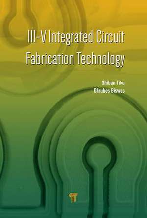
III-V Integrated Circuit Fabrication Technology
Editat de Shiban Tiku, Dhrubes Biswasen Limba Engleză Hardback – 11 mai 2016
Preț: 927.09 lei
Preț vechi: 1130.60 lei
-18% Nou
Puncte Express: 1391
Preț estimativ în valută:
177.42€ • 184.55$ • 146.47£
177.42€ • 184.55$ • 146.47£
Carte tipărită la comandă
Livrare economică 15-29 aprilie
Preluare comenzi: 021 569.72.76
Specificații
ISBN-13: 9789814669306
ISBN-10: 981466930X
Pagini: 716
Ilustrații: 364 Illustrations, color; 37 Illustrations, black and white
Dimensiuni: 152 x 229 x 38 mm
Greutate: 1.48 kg
Ediția:1
Editura: Jenny Stanford Publishing
Colecția Jenny Stanford Publishing
ISBN-10: 981466930X
Pagini: 716
Ilustrații: 364 Illustrations, color; 37 Illustrations, black and white
Dimensiuni: 152 x 229 x 38 mm
Greutate: 1.48 kg
Ediția:1
Editura: Jenny Stanford Publishing
Colecția Jenny Stanford Publishing
Public țintă
Academic and PostgraduateCuprins
Semiconductor fundamentals. GaAs devices. Phase diagrams and crystal growth. Epitaxy. Photolithography. Wet etching. Cleaning and passivation. Plasma processing and dry etching. Deposition. Ion implantation and device isolation. Diffusion. Ohmic contacts. Schottky diodes and FET processing. HEMT process. HBT processing. BiFET and BiHEMT processing. MOSFET processing. Passive components. Interconnect technology. Backside processing and wafer bumping. Electroplating. Measurements and characterization. Reliability. GaN devices and R F MEMs.
Notă biografică
Shiban Tiku is an electrical engineer from Kashmir University, India, an M. Tech. from IIT Kanpur, India, and a PhD in materials science from the University of Southern California, Los Angeles. Dr. Tiku started work in GaAs ICs at Texas Instruments, Dallas, and has been with the Rockwell Semiconductor Division, from which Skyworks, California, was spun off, for over 20 years, first in process development and then in process engineering and yield engineering, covering design, layout, wafer fabrication, and back-end processing. He has worked on epigrowth, ion implantation, thin-film deposition, FET- and HBT-type device processing, piezoelectric devices, etc., and is currently in charge of new process/product introduction at Skyworks. He has served on the CS MANTECH technical committee for over 10 years and is now on the executive committee as the university liaison. He has published numerous papers and is the (co)author of 15 patents.
Dhrubes Biswas is an electrical engineer from IIT Kharagpur, India, and an MS and PhD in engineering (electronic devices and materials) from the University of Illinois, Urbana-Champaign. Prof. Biswas has made significant contributions to gas-source molecular beam epitaxy and played an instrumental role in establishing and advising strategic technology ventures in wireless communication and optical networking electronics worldwide. Currently at IIT Kharagpur, he is the professor of electronics and electrical communication engineering and a professor at Rajendra Mishra School of Engineering Entrepreneurship. He is deeply involved in the integration of III–V electronics/optical front-end devices epitaxially on silicon for high-performance systems. He has authored over 170 technical papers and books and holds numerous patents. He is a senior member of the Institute of Electrical Engineers (IEEE) and a member of Tau Beta Pi and Phi Kappa Phi.
Dhrubes Biswas is an electrical engineer from IIT Kharagpur, India, and an MS and PhD in engineering (electronic devices and materials) from the University of Illinois, Urbana-Champaign. Prof. Biswas has made significant contributions to gas-source molecular beam epitaxy and played an instrumental role in establishing and advising strategic technology ventures in wireless communication and optical networking electronics worldwide. Currently at IIT Kharagpur, he is the professor of electronics and electrical communication engineering and a professor at Rajendra Mishra School of Engineering Entrepreneurship. He is deeply involved in the integration of III–V electronics/optical front-end devices epitaxially on silicon for high-performance systems. He has authored over 170 technical papers and books and holds numerous patents. He is a senior member of the Institute of Electrical Engineers (IEEE) and a member of Tau Beta Pi and Phi Kappa Phi.
Recenzii
"Drawing from decades of directly relevant experience in the field, the authors have created a modern, comprehensive review of all aspects of compound semiconductor IC fabrication, useful for both experts in the field and newcomers wanting to gain familiarity with the topic. This book contains extensive references, plus useful appendices of constants, acronyms, and material properties, making it a handy and often-pulled-off-the-shelf resource for CS professionals."
—Dr. Martin J. Brophy, Senior GaAs Test, Reliability, and Development Engineer, Avago Technologies
"This book will be greatly appreciated by researchers and students engaged in work with III–V semiconductors. With the primary focus on GaAs-based HBTs and related devices, the book also describes critical issues for emerging technologies such as GaN and RF MEMS. It brings together process information and insights from widely dispersed sources and provides a physics and chemistry background, along with up-to-date process design considerations, meeting several important needs of the III–V fabrication community."
—Prof. Peter Asbeck, Department of Electrical and Computer Engineering, University of California
Descriere
This book covers semiconductor material basics, physics of devices used in semiconductor integrated circuit processing, and all the processing technologies used in III–V semiconductor fabrication. The content is chosen according to the needs of students as seen by a teacher and needs of practicing engineers dealing with processing issues as seen by an experienced process engineer. The book covers all aspects of the current state of the art of III–V processing with emphasis on heterojunction bipolar transistors, the volume leader technology, having grown due to the explosive growth of wireless technology.
