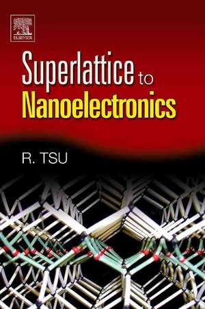
Superlattice to Nanoelectronics
Autor Raphael Tsuen Limba Engleză Hardback – 3 apr 2005
* The Author is one of the founders of the field of superlattices* The FIRST historical overview of the field* Provides a basic understanding of the physics involved from first principles, whilst adding new depth, using simple mathematics and explanation of the background essentials
Preț: 780.84 lei
Preț vechi: 1069.65 lei
-27% Nou
Puncte Express: 1171
Preț estimativ în valută:
149.41€ • 162.81$ • 125.90£
149.41€ • 162.81$ • 125.90£
Carte tipărită la comandă
Preluare comenzi: 021 569.72.76
Specificații
ISBN-13: 9780080443775
ISBN-10: 008044377X
Pagini: 325
Dimensiuni: 156 x 234 mm
Editura: ELSEVIER SCIENCE
ISBN-10: 008044377X
Pagini: 325
Dimensiuni: 156 x 234 mm
Editura: ELSEVIER SCIENCE
Public țintă
Academics, researchers and industry professionals working in nanoelectronics, materials science and electrical engineeringCuprins
Preface
Introduction
CHAPTER 1
SUPERLATTICE
1.1 The Birth of the Man-Made Superlattice
1.2 A Model for the Creation of Man-Made Energy Bands
1.3 Transport Properties of a Superlattice 6
1.4 More Rigorous Derivation of the Negative
Differential Conductance
1.5 Response of a Time-Dependent Electric Field
1.6 NDC from the Hopping Model and Electric Field
Induced Localization
1.7 Experiments
1.8 Type II Superlattice
1.9 Physical Realization and Characterization of a Superlattice
1.10 Summary
References
CHAPTER 2
RESONANT TUNNELING VIA MAN-MADE QUANTUM WELL STATES
2.1 The Birth of Resonant Tunneling
2.2 Some Fundamentals
2.3 Conductance from the Tsu–Esaki Formula
2.4 Tunneling Time from the Time-Dependent Schro¨dinger Equation
2.5 Damping in Resonant Tunneling
2.6 Very Short ‘ and w for an Amorphous Quantum Well
2.7 Self-Consistent Potential Correction of DBRT
2.8 Experimental Confirmation of Resonant Tunneling
2.9 Instability in RTD
2.10 Summary
References
CHAPTER 3
OPTICAL PROPERTIES AND RAMAN SCATTERING IN MAN-MADE QUANTUM SYSTEMS
3.1 Optical Absorption in a Superlattice
3.2 Photoconductivity in a Superlattice
3.3 Raman Scattering in a Superlattice and Quantum Well
3.4 Summary
References
CHAPTER 4
DIELECTRIC FUNCTION AND DOPING OF A SUPERLATTICE
4.1 Dielectric Function of a Superlattice and a Quantum Well
4.2 Doping a Superlattice
4.3 Summary
References
CHAPTER 5
QUANTUM STEP AND ACTIVATION ENERGY
5.1 Optical Properties of Quantum Steps
5.2 Determination of Activation Energy in Quantum Wells
5.3 Summary
References
CHAPTER 6
SEMICONDUCTOR ATOMIC SUPERLATTICE (SAS)
6.1 Silicon-Based Quantum Wells
6.2 Si-Interface Adsorbed Gas (IAG) Superlattice
6.3 Amorphous Silicon/Silicon Oxide Superlattice
6.4 Silicon–Oxygen (Si–O) Superlattice
6.5 Estimate of the Band-Edge Alignment Using Atomic States
6.6 Estimate of the Band-Edge Alignment with HOMO–LUMO
6.7 Estimation of Strain from a Ball and Stick Model
6.8 Electroluminescence and Photoluminescence
6.9 Transport through a Si–O Superlattice
6.10 Comparison of a Si–O Superlattice and a Ge–Si Monolayer Superlattice
6.11 Summary
References
CHAPTER 7
Si QUANTUM DOTS
7.1 Energy States of Silicon Quantum Dots
7.2 Resonant Tunneling in Silicon Quantum Dots
7.3 Slow Oscillations and Hysteresis
7.4 Avalanche Multiplication from Resonant Tunneling
7.5 Influence of Light and Repeatability under Multiple Scans
7.6 Summary
References
CHAPTER 8
CAPACITANCE, DIELECTRIC CONSTANT AND DOPING
QUANTUM DOTS
8.1 Capacitance of Silicon Quantum Dots
8.2 Dielectric Constant of a Silicon Quantum Dot
8.3 Doping a Silicon Quantum Dot
8.4 Summary
References
CHAPTER 9
POROUS SILICON
9.1 Porous Silicon—Light Emitting Silicon
9.2 Porous Silicon—Other Applications
9.3 Summary
References
CHAPTER 10
SOME NOVEL DEVICES
10.1 Cold Cathode
10.2 Saturation Intensity of PbS Quantum Dots
10.3 Multipole Electrode Heterojunction Hybrid Structures
10.4 Some Fundamental Issues: Mainly Difficulties
10.5 Comments on Quantum Computing
10.6 Summary
References
CHAPTER 11
QUANTUM IMPEDANCE OF ELECTRONS
11.1 Landauer Conductance Formula
11.2 Electron Quantum Waveguide (EQW)
11.3 Wave Impedance of Electrons
11.4 Summary
References
CHAPTER 12
NANOELECTRONICS: WHERE ARE YOU?
References
