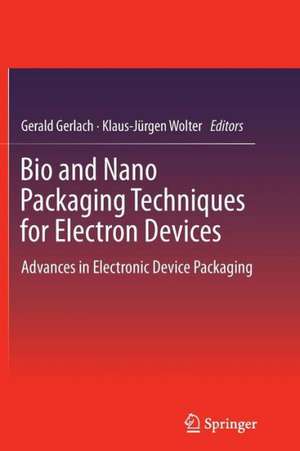
Bio and Nano Packaging Techniques for Electron Devices: Advances in Electronic Device Packaging
Editat de Gerald Gerlach, Klaus-Jürgen Wolteren Limba Engleză Paperback – 9 aug 2014
| Toate formatele și edițiile | Preț | Express |
|---|---|---|
| Paperback (1) | 713.69 lei 6-8 săpt. | |
| Springer Berlin, Heidelberg – 9 aug 2014 | 713.69 lei 6-8 săpt. | |
| Hardback (1) | 965.52 lei 6-8 săpt. | |
| Springer Berlin, Heidelberg – 17 iul 2012 | 965.52 lei 6-8 săpt. |
Preț: 713.69 lei
Preț vechi: 839.63 lei
-15% Nou
Puncte Express: 1071
Preț estimativ în valută:
136.57€ • 146.03$ • 113.86£
136.57€ • 146.03$ • 113.86£
Carte tipărită la comandă
Livrare economică 17 aprilie-01 mai
Preluare comenzi: 021 569.72.76
Specificații
ISBN-13: 9783642442865
ISBN-10: 3642442862
Pagini: 640
Ilustrații: XII, 628 p.
Dimensiuni: 155 x 235 x 34 mm
Greutate: 0.89 kg
Ediția:2012
Editura: Springer Berlin, Heidelberg
Colecția Springer
Locul publicării:Berlin, Heidelberg, Germany
ISBN-10: 3642442862
Pagini: 640
Ilustrații: XII, 628 p.
Dimensiuni: 155 x 235 x 34 mm
Greutate: 0.89 kg
Ediția:2012
Editura: Springer Berlin, Heidelberg
Colecția Springer
Locul publicării:Berlin, Heidelberg, Germany
Public țintă
ResearchCuprins
General Aspects.- 3D Modelling and Design for Nems.- Nanoparticles.- Nanopatterning.- Metallization.- Nano- and Bio-Functionalized Surfaces.- Biocompatible Packaging.- Thermal Management.- System-In-Package For Mems and Moems.
Notă biografică
Prof. Dr.-Ing. habil. Gerald Gerlach:
1983, 1987 Diploma and doctoral degree in EE from Technische Universität Dresden, Germany, respectively R&D engineer in measuring devices industry. Since 1993 Professor for Microtechnology, since 1996 Professor for Solid State Electronics in EE department of TU Dresden. 2001/02 Visiting professor at UCLA. Since 2002 Member of the Executive of VDE (German Association of Engineers in Electrical Engineering, Electronics, Information Technology). Since 2007 Chairperson of the German Society for Measurement and Automatic Control (GMA). Since 1996 Conference Chairman of the biannually organised International Conference „Infrared Sensors and Systems IRS2" in Nuremberg (in conjunction with the world’s largest sensor exhibition "Sensor+Test"). 2008 General Chairman of the Eurosensors XXII Conference, Dresden. Author and Co-author of some 280 scientific journal and international conference papers, holds more than 40 patents.Prof. Dr.-Ing. habil. Klaus-Juergen Wolter: 1967-1973 Studies in Control Theory at the Technical University Kiev, Ukraine. 1983 Dissertation "Correlation method for vision systems in microelectronics assembly". 1987 University Teaching Qualification (Habilitation). 1989-1973 R&D position the microelectronics industry. 1989 Assistant professor at the Institute of Electronic Technology. 1992 Appointment as Chair of Procedure Technology of Electronics. 1998 – 1999 Sabbatical at Tessera, San Jose, CA, (Wafer-Level-Packaging). Since 2002 Director of the Centre of Microtechnical Manufacturing (ZµP) at TUD. Since 2003 Director of the Electronic Packaging Lab at Dresden University of Technology. Since 2006 Deputy Head at Fraunhofer Institute IZFP Dresden.
Fields of research: Substrate technologies, Assembly technologies of devices, components, MEMS, Joining technologies, Reliability of electronic packages, Non-destructive test methods
Textul de pe ultima copertă
The book offers a comprehensive discussion of future trends and developments in electron device packaging and the opportunities of nano and bio techniques as future solutions. It describes effects of nano-sized particles and cell-based approaches for packaging solutions with their diverse requirements. It offers a comprehensive overview of nano particles and nano composites and their opportunities for packaging functions in electron devices. The importance and challenges of three-dimensional design and computer modeling in nano packaging is discussed and also shows ways for implementation. Solutions for unconventional packaging solutions for metallizations and functionalized surfaces are demonstrated. Also new packaging technologies with high potential for industrial applications like nano partical fabrication and application, nano imprinting and ink-jet printing are discussed. The book brings together a comprehensive overview of nano scale components and systems comprising electronic, mechanical and optical structures and serves as important reference for industrial and academic researchers as well as practicing engineers seeking information about the latest nano and bio techniques in packaging.
Caracteristici
Provides solutions for electron device packaging Comprehensive review of nanoscale materials for packaging Lists the future trends in nanobiotechniques Includes supplementary material: sn.pub/extras
