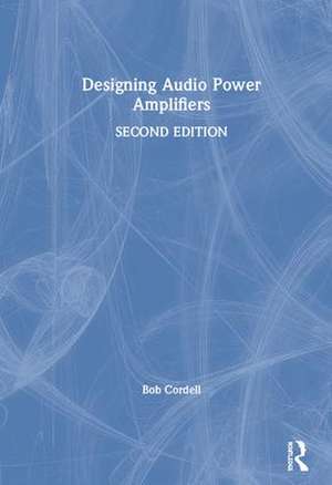
Designing Audio Power Amplifiers
Autor Bob Cordellen Limba Engleză Hardback – 10 iun 2019
Develop and hone your audio amplifier design skills with in-depth coverage of these and other topics:
- Basic and advanced audio power amplifier design
- Low-noise amplifier design
- Static and dynamic crossover distortion demystified
- Understanding negative feedback and the controversy surrounding it
- Advanced NFB compensation techniques, including TPC and TMC
- Sophisticated DC servo design
- MOSFET power amplifiers and error correction
- Audio measurements and instrumentation
- Overlooked sources of distortion
- SPICE simulation for audio amplifiers, including a tutorial on LTspice
- SPICE transistor modeling, including the VDMOS model for power MOSFETs
- Thermal design and the use of ThermalTrak™ transistors
- Four chapters on class D amplifiers, including measurement techniques
- Professional power amplifiers
- Switch-mode power supplies (SMPS).
| Toate formatele și edițiile | Preț | Express |
|---|---|---|
| Paperback (1) | 507.35 lei 3-5 săpt. | +48.71 lei 10-14 zile |
| Taylor & Francis – 13 iun 2019 | 507.35 lei 3-5 săpt. | +48.71 lei 10-14 zile |
| Hardback (1) | 1369.97 lei 6-8 săpt. | |
| Taylor & Francis – 10 iun 2019 | 1369.97 lei 6-8 săpt. |
Preț: 1369.97 lei
Preț vechi: 1712.46 lei
-20% Nou
Puncte Express: 2055
Preț estimativ în valută:
262.14€ • 274.43$ • 216.91£
262.14€ • 274.43$ • 216.91£
Carte tipărită la comandă
Livrare economică 05-19 aprilie
Preluare comenzi: 021 569.72.76
Specificații
ISBN-13: 9781138555457
ISBN-10: 1138555452
Pagini: 792
Ilustrații: 454
Dimensiuni: 178 x 254 x 47 mm
Greutate: 1.56 kg
Ediția:Nouă
Editura: Taylor & Francis
Colecția Routledge
Locul publicării:Oxford, United Kingdom
ISBN-10: 1138555452
Pagini: 792
Ilustrații: 454
Dimensiuni: 178 x 254 x 47 mm
Greutate: 1.56 kg
Ediția:Nouă
Editura: Taylor & Francis
Colecția Routledge
Locul publicării:Oxford, United Kingdom
Public țintă
General, Professional, and Professional ReferenceCuprins
Part 1: Audio Power Amplifier Basics
1. Introduction
1.1 Organization of the Book
1.2 The Role of the Power Amplifier
1.3 Basic Performance Specifications
1.4 Additional Performance Specifications
1.5 Output Voltage and Current
1.6 Basic Amplifier Topology
1.7 Summary
2. Power Amplifier Basics
2.1 BJT Transistors
2.2 JFETs
2.3 Power MOSFETs
2.4 Basic Amplifier Stages
2.5 Current Mirrors
2.6 Current Sources and Voltage References
2.7 Complementary Feedback Pair (CFP)
2.8 Vbe Multiplier
2.9 Operational Amplifiers
2.10 Amplifier Design Analysis
3. Power Amplifier Design Evolution
3.1 About Simulation
3.2 The Basic Power Amplifier
3.3 Adding Input Stage Degeneration
3.4 Adding a Darlington VAS
3.5 Input Stage Current Mirror Load
3.6 The Output Triple
3.7 Cascoded VAS
3.8 Paralleling Output Transistors
3.9 Higher Power Amplifiers
3.10 Crossover Distortion
3.11 Performance Summary
3.12 Completing an Amplifier
3.13 Summary
4. Building an Amplifier
4.1 The Basic Design
4.2 The Front-End: IPS, VAS and Pre-Drivers
4.3 Output Stage: Drivers and Outputs
4.4 Heat Sink and Thermal Management
4.5 Protection Circuits
4.6 Power Supply
4.7 Grounding
4.8 Building the Amplifier
4.9 Testing the Amplifier
4.10 Troubleshooting
4.11 Performance
4.12 Scaling
4.13 Upgrades
5. Noise
5.1. Signal-to-Noise Ratio
5.2. A-weighted Noise Specifications
5.3 Noise Power and Noise Voltage
5.4 Noise Bandwidth
5.5 Noise Voltage Density and Spectrum
5.6 Relating Input Noise Density to Signal-to-Noise Ratio
5.7 Amplifier Noise Sources
5.8 Thermal Noise
5.9 Shot Noise
5.10 Bipolar Transistor Noise
5.11 JFET Noise
5.12. Op Amp Noise
5.13 Noise Simulation
5.14 Amplifier Circuit Noise
5.15 Excess Resistor Noise
5.16 Zener and LED Noise
6. Negative Feedback Compensation and Slew Rate
6.1 How Negative Feedback Works
6.2 Input-referred Feedback Analysis
6.3 Feedback Compensation and Stability
6.4 Feedback Compensation Principles
6.5 Evaluating Loop Gain
6.6 Evaluating Stability
6.7 Compensation Loop Stability
6.8 Slew Rate
7. Amplifier Classes, Output Stages and Efficiency
7.1 Class A, AB and B Operation
7.2 The Complementary Emitter Follower Output Stage
7.3 Output Stage Efficiency
7.4 Complementary Feedback Pair Output Stages
7.5 Stacked Output Stages
7.6 Classes G and H
7.7 Class D
8. Summary of Amplifier Design Considerations
8.1 Power and Loads
8.2 Sizing the Power Supply
8.3 Sizing the Output Stage
8.4 Sizing the Heat Sink
8.5 Protecting the Amplifier and Loudspeaker
8.6 Power and Ground Distribution
8.7 Other Considerations
Part 2: Advanced Power Amplifier Design
9. Input and VAS Circuits
9.1 Single-Ended IPS-VAS
9.2 JFET Input Stages
9.3 Buffered Input Stages
9.4 CFP Input Stages
9.5 Complementary IPS and Push-Pull VAS
9.6 Unipolar Input Stage and Push-Pull VAS
9.7 Input Common Mode Distortion
9.8 Early Effect
9.9 Baker Clamps
9.10 Current Feedback Amplifiers
9.11 Example IPS/VAS
10. DC Servos
10.1 Origins and Consequences of DC Offset
10.2 DC Servo Basics
10.3 The Servo Is in the Signal Path
10.4 DC Offset Detection and Protection
10.5 DC Servo Example
10.6 Eliminating the Input Coupling Capacitor
10.7 DC Servo Design Issues and Nuances
11. Advanced Forms of Feedback Compensation
11.1 Understanding Stability Issues
11.2 Miller Compensation
11.3 Miller Input Compensation
11.4 Two-Pole Compensation
11.5 Transitional Miller Compensation
11.6 A Vertical MOSFET TMC Amplifier Example
11.7 Conclusion
12. Output Stage Design and Crossover Distortion
12.1 The Class AB Output Stage
12.2 Static Crossover Distortion
12.3 Optimum Bias and Bias Stability
12.4 Output Stage Driver Circuits
12.5 Output Transistor Matching Considerations
12.6 Dynamic Crossover Distortion
12.7 The Output Emitter Resistors
12.8 Output Networks
12.9 Output Stage Frequency Response and Stability
12.10 Sizing the Output Stage
12.11 Delivering High Current
12.12 Driving Paralleled Output Stages
12.13 Advanced Output Transistors
13. Output Stages II
13.1. VAS Output Impedance and Stability
13.2. Complementary Feedback Pair
13.3 Output Stages with Gain
13.4 Bryston Output Stage
13.5 ThermalTrak™ Output Stage
13.6 Class A Output Stage
13.7 Crossover Displacement (Class XD™)
13.8 Double Cross™ Output Stage
13.9 Sliding Bias and Non-switching Output Stages
13.10 LT1166 Output Stage
13.11 Measuring Output Stage Distortion
13.12 Setting the Bias
14. MOSFET Power Amplifiers
14.1 MOSFET Types and Characteristics
14.2 MOSFET Advantages and Disadvantages
14.3 Lateral vs. Vertical Power MOSFETs
14.4 Parasitic Oscillations
14.5 Biasing Power MOSFETs
14.6 Crossover Distortion
14.7 Driving Power MOSFETs
14.8 Paralleling and Matching MOSFETs
14.9 Simulating MOSFET Power Amplifiers
14.10 A Lateral MOSFET Power Amplifier Design
14.11 A Vertical MOSFET Power Amplifier Design
15. Error Correction
15.1 Feedforward Error Correction
15.2 Hawksford Error Correction
15.3 Error Correction for MOSFET Output Stages
15.4 Stability and Compensation
15.5 Performance and Design Issues
15.6 Circuit Refinements and Nuances
15.7 A MOSFET Power Amplifier with Error Correction
16. Other Sources of Distortion
16.1 Distortion Mechanisms
16.2 Early Effect Distortion
16.3 Junction Capacitance Distortion
16.4 Grounding Distortion
16.5 Power Rail Distortion
16.6 Input Common Mode Distortion
16.7 Resistor Distortion
16.8 Capacitor Distortion
16.9 Inductor and Magnetic Distortions
16.10 Magnetic Induction Distortion
16.11 Fuse, Relay and Connector Distortion
16.12 Load Induced Distortion
16.13 EMI-Induced Distortion
16.14 Thermally Induced Distortion (Memory Distortion)
Part 3: Real World Design Considerations
17. Output Stage Thermal Design and Stability
17.1 Power Dissipation vs. Power and Load
17.2 Thermal Design Concepts and Thermal Models
17.3 Transistor Power Ratings
17.4 Sizing the Heat Sink
17.5 The Bias Spreader and Temperature Compensation
17.6 Thermal Bias Stability
17.7 Thermal Lag Distortion
17.8 ThermalTrak™ Power Transistors
17.9 A ThermalTrak™ Power Amplifier
18. Safe Area and Short Circuit Protection
18.1 Power Transistor Safe Operating Area
18.2 Output Stage Safe Operating Area
18.3 Short Circuit Protection
18.4 Safe Area Limiting Circuits
18.5 Testing Safe Area Limiting Circuits
18.6 Protection Circuits for MOSFETs
18.7 Protecting the Driver Transistors
18.8 Loudspeaker Protection Circuits
19. Power Supplies and Grounding
19.1 The Design of the Power Supply
19.2 Sizing the Transformer
19.3 Sizing the Rectifier
19.4 Sizing the Reservoir Capacitors
19.5 Rectifier Speed
19.6 Regulation and Active Smoothing of the Supply
19.7 SPICE Simulation of Power Supplies
19.8 Soft-Start Circuits
19.9 Grounding Architectures
19.10 Radiated Magnetic Fields
19.11 Safety Circuits
19.12 DC on the Mains
19.13 Switching Power Supplies
20. Switching Power Supplies
20.1 Line DC Supply
20.2 Isolated DC-DC Converter
20.3 Buck Converters
20.4 Synchronous Buck Converter
20.5 Boost Converters
20.6 Buck-Boost Converters
20.7 Boost-Buck Converters
20.8 Cuk Converters
20.9 Forward Converters
20.10 Flyback Converters
20.11 Half-bridge Converters
20.12 Full-bridge Converters
20.13 Control ICs for PWM Converters
20.14 Resonant Converters
20.15 Quasi-Resonant Converters
20.16 EMI Filtering and Suppression
20.17 Power Factor Correction
20.18 Auxiliary Supplies
20.19 Switching Supplies for Power Amplifiers
20.20 Switching Supplies for Class D Amplifiers
21. Clipping Control and Civilized Amplifier Behavior
21.1 The Incidence of Clipping
21.2 Clipping and Sticking
21.3 Negative Feedback and Clipping
21.4 Baker Clamps
21.5 Soft Clipping
21.6 Current Limiting
21.7 Parasitic Oscillation Bursts
21.8 Selectable Output Impedance
22. Interfacing the Real World
22.1 The Amplifier-Loudspeaker Interface
22.2 EMI Ingress – Antennas Everywhere
22.3 Input Filtering
22.4 Input Ground Loops
22.5 Mains Filtering
22.6 EMI Egress
22.7 EMI Susceptibility Testing
Part 4: Simulation and Measurement
23. SPICE Simulation
23.1 Linear Technologies LTspice®
23.2 Schematic Capture
23.3 DC, AC and Transient Simulation
23.4 Distortion Analysis
23.5 Noise Analysis
23.6 Controlled Voltage and Current Sources
23.7 Swept and Stepped Simulations
23.8 Plotting Results
23.9 Subcircuits
23.10 SPICE Models
23.11 Simulating a Power Amplifier
23.12 Middlebrook and Tian Probes
24. SPICE Models and Libraries
24.1 Verifying SPICE Models
24.2 Tweaking SPICE Models
24.3 Creating a SPICE Model
24.4 JFET Models
24.5 Vertical Power MOSFET Models
24.6 LTspice VDMOS Models
24.7 The EKV Model
24.8 Lateral Power MOSFETs
24.9 Installing Models
25. Audio Instrumentation
25.1 Basic Audio Test Instruments
25.2 Dummy Loads
25.3 Simulated Loudspeaker Loads
25.4 THD Analyzer
25.5 PC-Based Instruments
25.6 Purpose-Built Test Gear
26. Distortion and its Measurement
26.1 Nonlinearity and its Consequences
26.2 Total Harmonic Distortion
26.3 SMPTE IM
26.4 CCIF IM
26.5 Transient Intermodulation Distortion (TIM) and SID
26.6 Phase Intermodulation Distortion (PIM)
26.7 Interface Intermodulation Distortion (IIM)
26.8 Multi-Tone Intermodulation Distortion (MIM)
26.9 Highly Sensitive Distortion Measurement
26.10 Input-Referred Distortion Analysis
27. Other Amplifier Tests
27.1 Measuring Damping Factor
27.2 Sniffing Parasitic Oscillations
27.3 EMI Ingress Susceptibility
27.4 Burst Power and Peak Current
27.5 PSRR Tests
27.6 Low-frequency Tests
27.7 Back-Feeding Tests
Part 5: Topics in Amplifier Design
28. The Negative Feedback Controversy
28.1 How Negative Feedback Got its Bad Rap
28.2 Negative Feedback and Open-loop Bandwidth
28.3 Spectral Growth Distortion
28.4 Global Versus Local Feedback
28.5 Timeliness of Correction
28.6 EMI from the Speaker Cable
28.7 Stability and Burst Oscillations
28.8 Clipping Behavior
29. Amplifiers without Negative Feedback
29.1 Design Tradeoffs and Challenges
29.2 Additional Design Techniques
29.3 An Example Design with No Feedback
29.4 A Feedback Amplifier with Wide Open-loop Bandwidth
30. Balanced and Bridged Amplifiers
30.1 Balanced Input Amplifiers
30.2 Bridged Amplifiers
30.3 Balanced Amplifiers
31. Integrated Circuit Power Amplifiers and Drivers
31.1 IC Power Amplifiers
31.2 The Gain Clones
31.3 The Super Gain Clone
31.4 Integrated Circuit Drivers
31.5 Summary
32. Professional Power Amplifiers
32.1 Environment and Special Needs
32.2 Output Stages and Output Power
32.3 Power Supplies
32.4 Cooling and Heat Removal
32.5 Microcomputers
32.6 Networked Control and Monitoring
32.7 Digital Signal Processing
32.8 DSP-Based Protection and Monitoring
32.9 The DSP to Class D Interface
32.10 Programming
32.11 Audio Networking
Part 6: Class D Audio Amplifiers
33. Class D Audio Amplifiers
33.1 How Class D Amplifiers Work
33.2 Class D Output Stages
33.3 Bridge Tied Load Designs
33.4 Negative Feedback
33.5 Noise Shaping in PWM Modulators with Feedback
33.6 Summary
34. Class D Design Issues
34.1 The Output Filter and EMI
34.2 Spread Spectrum Class D
34.3 Filterless Class D Amplifiers
34.4 Buck Converters and Class D Amplifiers
34.5 Sources of Distortion
34.6 Bus Pumping
34.7 Power Supply Rejection
34.8 Power Supplies for Class D Amplifiers
34.9 Damping Factor and Load Invariance
34.10 Summary
35. Alternative Class D Modulators
35.1 Self-Oscillating Loops
35.2 Sigma-Delta Modulators
35.3 Digital Modulators
36. Class D Measurement, Efficiency and Designs
36.1 Hybrid Class D
36.2 Measuring Class D Amplifiers
36.3 Achievable Performance
36.4 Integrated Circuits for Class D Amplifiers
36.5 Example Class D Amplifiers and Measurements
Notă biografică
Bob Cordell is an electrical engineer who has been deeply involved in audio since his adventures with vacuum tube designs in his teen years. He is an equal-opportunity designer to this day, having built amplifiers with vacuum tubes, bipolar transistors and MOSFETs. Bob is also a prolific designer of audio test equipment, including a high-performance THD analyzer and many purpose-built pieces of audio gear. He has published numerous articles and papers on power amplifier design and distortion measurement in the popular press and in the Journal of the Audio Engineering Society. In 1983 he published a power amplifier design combining vertical power MOSFETs with error correction, achieving unprecedented distortion levels of less than 0.001% at 20 kHz. He also consults in the audio and semiconductor industries.
Bob is also an avid DIY loudspeaker builder, and has combined this endeavor with his electronic interests in the design of powered audiophile loudspeaker systems. Bob and his colleagues have presented audiophile listening and measurement workshops at the Rocky Mountain Audio Fest and the Home Entertainment Show.
As an Electrical Engineer, Bob has worked at Bell Laboratories and other related telecommunications companies, where his work has included design of integrated circuits and fiber optic communications systems. Bob maintains an audiophile website at www.cordellaudio.com where diverse material on audio electronics, loudspeakers and instrumentation can be found.
Recenzii
"Essential reading for anyone fascinated by the superficially simple idea of how to make a small electrical signal powerful enough to drive a loudspeaker without degrading that signal in the process." - John Atkinson, Stereophile
"A complete text ideal for newcomers to amplifier design engineering as well as a great reference for practicing audio design engineers already working in the industry. [...] Because of the tiered approach of the first three parts of the book, its usefulness will grow with you as you become more proficient at amplifier design. I’m happy to find a place for this book in my technical library, as should you." - Dennis Fink, Fink Analog Audio, Journal of the Audio Engineering Society
"A complete text ideal for newcomers to amplifier design engineering as well as a great reference for practicing audio design engineers already working in the industry. [...] Because of the tiered approach of the first three parts of the book, its usefulness will grow with you as you become more proficient at amplifier design. I’m happy to find a place for this book in my technical library, as should you." - Dennis Fink, Fink Analog Audio, Journal of the Audio Engineering Society
Descriere
This comprehensive book on audio power amplifier design will appeal to members of the professional audio engineering community as well as the student and enthusiast.
