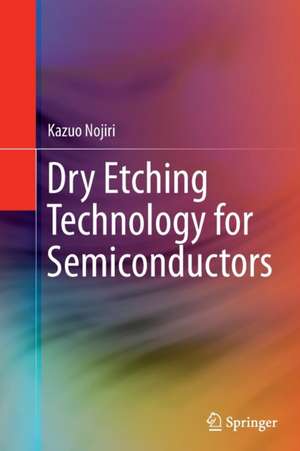
Dry Etching Technology for Semiconductors
Autor Kazuo Nojirien Limba Engleză Paperback – 10 sep 2016
| Toate formatele și edițiile | Preț | Express |
|---|---|---|
| Paperback (1) | 632.37 lei 6-8 săpt. | |
| Springer International Publishing – 10 sep 2016 | 632.37 lei 6-8 săpt. | |
| Hardback (1) | 888.18 lei 6-8 săpt. | |
| Springer International Publishing – 3 noi 2014 | 888.18 lei 6-8 săpt. |
Preț: 632.37 lei
Preț vechi: 743.97 lei
-15% Nou
Puncte Express: 949
Preț estimativ în valută:
121.01€ • 126.92$ • 100.73£
121.01€ • 126.92$ • 100.73£
Carte tipărită la comandă
Livrare economică 01-15 aprilie
Preluare comenzi: 021 569.72.76
Specificații
ISBN-13: 9783319356242
ISBN-10: 3319356240
Pagini: 129
Ilustrații: XIII, 116 p. 123 illus.
Dimensiuni: 155 x 235 x 7 mm
Greutate: 0.2 kg
Ediția:Softcover reprint of the original 1st ed. 2015
Editura: Springer International Publishing
Colecția Springer
Locul publicării:Cham, Switzerland
ISBN-10: 3319356240
Pagini: 129
Ilustrații: XIII, 116 p. 123 illus.
Dimensiuni: 155 x 235 x 7 mm
Greutate: 0.2 kg
Ediția:Softcover reprint of the original 1st ed. 2015
Editura: Springer International Publishing
Colecția Springer
Locul publicării:Cham, Switzerland
Cuprins
Contribution of Dry Etching Technology to Progress of Semiconductor Integrated Circuit.- Mechanism of Dry Etching.- Dry Etching of Various Materials.- Dry Etching Equipments.- Dry Etching Damage.- Latest Dry Etching Technologies.- Future Challenges and Outlook for Dry Etching Technology.
Notă biografică
Kazuo Nojiri is a CTO of Lam Research Japan. He has 37 years of experience in semiconductor industry. Prior to joining Lam in 2000, he worked for Hitachi Ltd. for 25 years, where he held numerous management positions for Dry Etching and Device Integration. He is also known as a pioneer in the research field of charging damage. He published 38 technical papers and 3 books. In 1984 he was awarded the Okouchi Memorial Prize for the development of ECR plasma etching technology.
Textul de pe ultima copertă
This book is a must-have reference to dry etching technology for semiconductors, which will enable engineers to develop new etching processes for further miniaturization and integration of semiconductor integrated circuits. The author describes the device manufacturing flow, and explains in which part of the flow dry etching is actually used. The content is designed as a practical guide for engineers working at chip makers, equipment suppliers and materials suppliers, and university students studying plasma, focusing on the topics they need most, such as detailed etching processes for each material (Si, SiO2, Metal etc) used in semiconductor devices, etching equipment used in manufacturing fabs, explanation of why a particular plasma source and gas chemistry are used for the etching of each material, and how to develop etching processes. The latest, key technologies are also described, such as 3D IC Etching, Dual Damascene Etching, Low-k Etching, Hi-k/Metal Gate Etching, FinFET Etching, Double Patterning etc.
- Provides a comprehensive, systematic guide to dry etching technologies, from basics to latest technologies;
- Enables beginners to understand the mechanisms of dry etching, without complexities of numerical formulas/equations;
- Describes etching processes for all materials which are used in semiconductor devices, explains key etching parameters for each material, and explains why a particular plasma source and etching gas chemistry is used for each material;
- Discusses the device manufacturing flow and explains in which part of device manufacturing dry etching is actually used;
- Describes the types and plasma generation mechanism of etching equipment which are actually used in semiconductor fabs, such as CCP (Capacitively Coupled Plasma), Magnetron RIE (Magnetron Reactive Ion Etching), ECR (Electron Cyclotron Resonance) Plasma, and ICP (Inductively Coupled Plasma).
Caracteristici
Provides a comprehensive, systematic guide to dry etching technologies, from basics to latest technologies Enables beginners to understand the mechanisms of dry etching, without complexities of numerical formulas/equations Describes etching processes for all materials which are used in semiconductor devices, explains key etching parameters for each material, and explains why a particular plasma source and etching gas chemistry is used for each material Discusses the device manufacturing flow and explains in which part of device manufacturing dry etching is actually used Describes the types and plasma generation mechanism of etching equipment which are actually used in semiconductor fabs, such as CCP (Capacitively Coupled Plasma), Magnetron RIE (Magnetron Reactive Ion Etching), ECR (Electron Cyclotron Resonance) Plasma, and ICP (Inductively Coupled Plasma) Includes supplementary material: sn.pub/extras
