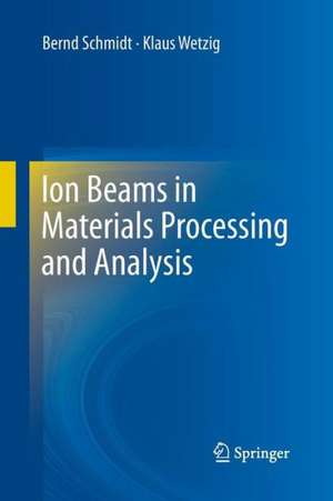
Ion Beams in Materials Processing and Analysis
Autor Bernd Schmidt, Klaus Wetzigen Limba Engleză Paperback – 27 noi 2014
| Toate formatele și edițiile | Preț | Express |
|---|---|---|
| Paperback (1) | 1114.21 lei 6-8 săpt. | |
| SPRINGER VIENNA – 27 noi 2014 | 1114.21 lei 6-8 săpt. | |
| Hardback (1) | 1126.52 lei 6-8 săpt. | |
| SPRINGER VIENNA – 12 dec 2012 | 1126.52 lei 6-8 săpt. |
Preț: 1114.21 lei
Preț vechi: 1358.78 lei
-18% Nou
Puncte Express: 1671
Preț estimativ în valută:
213.21€ • 227.99$ • 177.77£
213.21€ • 227.99$ • 177.77£
Carte tipărită la comandă
Livrare economică 18 aprilie-02 mai
Preluare comenzi: 021 569.72.76
Specificații
ISBN-13: 9783709117330
ISBN-10: 370911733X
Pagini: 428
Ilustrații: IX, 418 p.
Dimensiuni: 155 x 235 x 22 mm
Greutate: 0.6 kg
Ediția:2013
Editura: SPRINGER VIENNA
Colecția Springer
Locul publicării:Vienna, Austria
ISBN-10: 370911733X
Pagini: 428
Ilustrații: IX, 418 p.
Dimensiuni: 155 x 235 x 22 mm
Greutate: 0.6 kg
Ediția:2013
Editura: SPRINGER VIENNA
Colecția Springer
Locul publicării:Vienna, Austria
Public țintă
ResearchCuprins
Preface
1. Introduction
2. Fundamentals
3. Ion Beam Technology
3.1 Principles of Ion Accelerators
3.1.1 Low Energy Ion Accelerators (Ion Implanters)
3.1.2 High Energy Ion Accelerators
3.2 Ion Sources
3.2.1 Hot Filament (Hot Cathode) Ion Sources
3.2.2 Cold Cathode Ion Source (Penning Ion Source)
3.2.3 High Frequency (RF) Ion Source
3.2.4 Duoplasmatron Ion Source
3.2.5 Ion Sources for Electrostatic Accelerators
3.2.6 Cesium Sputtering Ion Sources
3.2.7 Field-Evaporation or Liquid Metal Ion Sources (LMIS)
3.2.8 Beam Extraction from Ion Sources
3.3 Ion Acceleration
3.4 Ion Beam Handling
3.4.1 Ion Mass Separation
3.4.2 Ion Beam Focusing
3.4.3 Ion Beam Scanning
3.4.4 Ion Beam Current Measurement
3.4.5 Ion Detection (Detectors, Spectrometers)
3.5 Ion Implantation Systems
3.5.1 Common Low Energy Beam Line Implanters
3.5.2 Specialized Low Energy Beam Line Implanters
3.5.3 High Energy Beam Line Implanters
3.5.4 Plasma Based Ion Implanters (PBII)
3.6 Electrostatic Ion Accelerator Systems
3.6.1 Single-Stage Electrostatic Accelerators
3.6.2 Two-Stage Electrostatic Accelerators
3.7 Focused Ion Beam Systems
3.7.1 Low Energy Focused Ion Beams
3.7.2 High Energy Focused Ion Beams
4. Materials Processing
4.1 Ion Irradiation and Damage Annealing
4.2 Ion Implantation into Semiconductors
4.2.1 Ion Implantation into Silicon
4.2.1.1 Advanced CMOS Technology
4.2.1.2 Defect Engineering and Epi-Layer Replacing in High Power Devices
4.2.1.3 Silicon Detector and Sensor Technology
4.2.2 Ion Implantation into Germanium
4.2.3 Ion Implantation into Compound Semiconductors
4.2.3.1 III-V Semiconductors
4.2.3.2 Group III-Nitride Materials
4.2.3.3 Silicon Carbide
4.3 Ion Beam Synthesis of New Phases in Solids
4.3.1 Buried Insulating Layers in Silcon
4.3.2 Ion Beam Synthesized Silicide Layers
4.3.3 Ion Beam Synthesis of Nanocrystals in Insulators
4.4 Ion Beam Mixing of Interfaces
4.5 Ion Beam Slicing of Thin Layers (Smart-Cut for SOI and Solar Cells)
4.6 Ion Beam Erosion, Sputtering and Surface Patterning (Ripples)
4.7 Ion Beam Shaping of Nanomaterials
4.8 Ion Beam Processing of other Materials (Metals, Insulators, Polymers...)
4.8.1 Ion Implantation of Metals
4.8.2 Ion Implantation into Polymers
4.8.3 Ion Implantation into Insulating Optical Materials
5. Ion Beam Preparation of Materials
5.1 Displacement of Target Atoms by Sputtering
5.2 Effects on Sputtering Yield
5.2.1 Ion Energy and Ion Atomic Number
5.2.2 Ion Incident Direction
5.2.3 Selective Sputtering
5.2.4 Targert Material
5.2.5 Preferential Sputtering
5.3 Ion Beam Induced Target Modifications
5.3.1 Ion Beam Cleaning and Etching
5.3.2 Ion Beam Induced Material Deposition
5.3.3 Ion Beam Depth Profiling
5.3.4 Ion Beam Cutting
5.3.5 Ion Beam Thinning
5.4 Focus Ion Beam (FIB) Preparation
5.4.1 FIB Induced Cross Section Preparation
5.4.2 FIB Induced Thin Film Preparation
5.4.3 Limiting Effects at FIB Preparation
6. Ion Beam Analysis of Materials
6.1 Ion- Solid State Interactions
6.2 Ion Beam Analytical Techniques – a Survey
6.3 Ion Beam Scattering Techniques
6.3.1 Rutherford Backscattering (RBS)
6.3.2 Medium Energy Ion Scattering (MEIS)
6.3.3 Elastic Recoil Detection Analysis (ERDA)
6.4 Ion Beam Induced Photon Emission
6.4.1 Particle Induced X-Ray Emission (PIXE)
6.4.2 Particle Induced γ-Ray Emission (PIGE)
6.5 Nuclear Reaction Analysis (NRA)
6.6 Ion Beam Induced Light and Electron Emission
6.7 Secondary Ion Emission
6.7.1 Dynamic Secondary Ion Mass Spectrometry (Dynamic SIMS)
6.7.2 Static Secondary Ion Mass Spectrometry (Static SIMS)
6.7.3 Sputtered Neutral Particle Mass Spectrometry (SNMS)
6.8 Ion Beam Imaging Techniques
6.8.1 Field Ion Microscopy
6.8.2 Ion Microscopy with Stationary Beam
6.8.3 Scanning Ion Microscopy
7. Special Ion Beam Applications in Materials Analysis Problems
7.1 Functional Thin Films and Layers
7.1.1 Direct Study of Diffusion Pricesses in Amorphous Thin Layer Systems
7.1.2 Nanoanalytical Investigations of Tunnelmagnetoresistance Layers
7.2 Ion Beam Analysis in Art and Archeometry
7.3 Special Applications in Life Sciences
Index
Notă biografică
Bernd Schmidt received his PhD in Physics at the State University of St. Petersburg (Russia) in 1976. Since 1994 he has been head of the Process Technology Division at the Helmholtz-Zentrum Dresden-Rossendorf, Germany. His research interests include semiconductor technology as well as ion implantation and the synthesis of nanostructures. He is author of the specialist book "Silicon Sensors" (1986) and of more than 150 refereed journal papers.
Klaus Wetzig received his PhD (1967) and postdoctoral (1973) degrees in Physics at the TU Dresden, Germany. From 1992 until his retirement in 2006 he was full professor of Materials Analysis at the TU Dresden and research director at the Leibniz Institute for Solid State and Materials Research Dresden (IFW). His research interests include materials analysis, nanostructures and particle-solid interactions. He is author of several specialist books and of more than 300 refereed journal papers.
Klaus Wetzig received his PhD (1967) and postdoctoral (1973) degrees in Physics at the TU Dresden, Germany. From 1992 until his retirement in 2006 he was full professor of Materials Analysis at the TU Dresden and research director at the Leibniz Institute for Solid State and Materials Research Dresden (IFW). His research interests include materials analysis, nanostructures and particle-solid interactions. He is author of several specialist books and of more than 300 refereed journal papers.
Textul de pe ultima copertă
A comprehensive review of ion beam application in modern materials research is provided, including the basics of ion beam physics and technology. The physics of ion-solid interactions for ion implantation, ion beam synthesis, sputtering and nano-patterning is treated in detail. Its applications in materials research, development and analysis, developments of special techniques and interaction mechanisms of ion beams with solid state matter result in the optimization of new material properties, which are discussed thoroughly. Solid-state properties optimization for functional materials such as doped semiconductors and metal layers for nano-electronics, metal alloys, and nano-patterned surfaces is demonstrated. The ion beam is an important tool for both materials processing and analysis. Researchers engaged in solid-state physics and materials research, engineers and technologists in the field of modern functional materials will welcome this text.
Caracteristici
Offers comprehensive treatment of the use of ion beams in material science research
Includes numerous tables, graphs and illustrations that amplify the text
Provides optimization strategies for solid-state properties of functional materials
Includes numerous tables, graphs and illustrations that amplify the text
Provides optimization strategies for solid-state properties of functional materials
