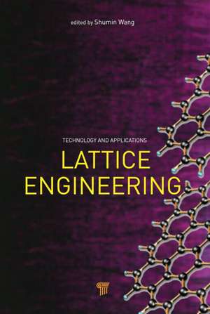
Lattice Engineering: Technology and Applications
Editat de Shumin Wangen Limba Engleză Hardback – 27 noi 2012
Preț: 657.17 lei
Preț vechi: 879.25 lei
-25% Nou
Puncte Express: 986
Preț estimativ în valută:
125.77€ • 130.82$ • 103.83£
125.77€ • 130.82$ • 103.83£
Carte tipărită la comandă
Livrare economică 14-28 aprilie
Preluare comenzi: 021 569.72.76
Specificații
ISBN-13: 9789814316293
ISBN-10: 9814316296
Pagini: 412
Ilustrații: 183 b/w images and 10 color images
Dimensiuni: 152 x 229 x 25 mm
Greutate: 0.69 kg
Ediția:1
Editura: Jenny Stanford Publishing
Colecția Jenny Stanford Publishing
ISBN-10: 9814316296
Pagini: 412
Ilustrații: 183 b/w images and 10 color images
Dimensiuni: 152 x 229 x 25 mm
Greutate: 0.69 kg
Ediția:1
Editura: Jenny Stanford Publishing
Colecția Jenny Stanford Publishing
Public țintă
Academic and PostgraduateCuprins
Dislocation Reduction by Interfacial Misfit Method. Compliant Substrates. Selective Area Growth. Low Temperature Direct Wafer Bonding. Heterostructures and Strain Relaxation In Semiconductor Nanowires. Epitaxial Growth of Nitrides. Metamorphic HEMT Technology. Metamorphic Hbts, Metamorphic Quantum Dot Lasers. Metamorphic Quantum Well Lasers. Nitride Based LEDS And Laser Diodes.
Notă biografică
Shumin Wang is Professor at Photonics Laboratory, Department of Microtechnology and Nanoscience, Chalmers University of Technology, Sweden. He received BSc and MSc from Department of Physics, Fudan University, China, in 1985 and 1988, respectively, and PhD from Department of Physics, Gothenburg University, Sweden, in 1994. He has been then working at Chalmers University of Technology, Sweden, since 1994, and was promoted to Associate Professor and Professor in 1999 and 2008, respectively.
Descriere
This book contains comprehensive reviews of different technologies to harness lattice mismatch in semiconductor heterostructures and their applications in electronic and optoelectronic devices. While the book is a bit focused on metamorphic epitaxial growth, it also includes other methods like compliant substrate, selective area growth, wafer bonding, heterostructure nanowires, and more. Basic knowledge on dislocations in semiconductors and innovative methods to eliminate threading dislocations are provided, and successful device applications are reviewed. It covers a variety of important semiconductor materials like SiGe, III-V including GaN and nano-wires; epitaxial methods like molecular beam epitaxy and metal organic vapor phase epitaxy; and devices like transistors and lasers etc.
