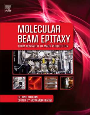
Molecular Beam Epitaxy: From Research to Mass Production
Editat de Mohamed Heninien Limba Engleză Paperback – 25 iun 2018
This second edition covers the advances made by MBE, both in research and in the mass production of electronic and optoelectronic devices. Enhancements include new chapters on MBE growth of 2D materials, Si-Ge materials, AIN and GaN materials, and hybrid ferromagnet and semiconductor structures.
- Condenses the fundamental science of MBE into a modern reference, speeding up literature review
- Discusses new materials, novel applications and new device structures, grounding current commercial applications with modern understanding in industry and research
- Includes coverage of MBE as mass production epitaxial technology and how it enhances processing efficiency and throughput for the semiconductor industry and nanostructured semiconductor materials research community
| Toate formatele și edițiile | Preț | Express |
|---|---|---|
| Paperback (1) | 1066.65 lei 5-7 săpt. | |
| ELSEVIER SCIENCE – 25 iun 2018 | 1066.65 lei 5-7 săpt. | |
| Hardback (1) | 948.39 lei 5-7 săpt. | |
| ELSEVIER SCIENCE – 31 dec 2012 | 948.39 lei 5-7 săpt. |
Preț: 1066.65 lei
Preț vechi: 1172.15 lei
-9% Nou
Puncte Express: 1600
Preț estimativ în valută:
204.13€ • 212.33$ • 168.52£
204.13€ • 212.33$ • 168.52£
Carte tipărită la comandă
Livrare economică 07-21 aprilie
Preluare comenzi: 021 569.72.76
Specificații
ISBN-13: 9780128121368
ISBN-10: 012812136X
Pagini: 788
Dimensiuni: 216 x 276 mm
Greutate: 1.8 kg
Ediția:2
Editura: ELSEVIER SCIENCE
ISBN-10: 012812136X
Pagini: 788
Dimensiuni: 216 x 276 mm
Greutate: 1.8 kg
Ediția:2
Editura: ELSEVIER SCIENCE
Public țintă
Materials Science and Physics researchersCuprins
1. Molecular beam epitaxy of transition metal monopnictides2. Migration Enhanced Epitaxy of Low Dimensional Structures3. MBE growth of Si-Ge materials and heterostructures4. SiGeSn MBE 5. MBE of Dilute Nitride Optoelectronic Devices6. Nonpolar Cubic III Nitrides: From the Basics of Growth to Device Applications7. AlGaN nanowires for deep ultraviolet optoelectronics8. plasma–assisted MBE of (Al,Ga)N layers and heterostructures 9. InAsBi and InAsSbBi materials10. Molecular beam epitaxy of GaAsBi and related quaternary alloys11. Molecular Beam Epitaxy of IV-VI Compounds: Heterostructures/Superlattices/Devices12. NIL-based site-control epitaxy13. Droplet epitaxy of nanostructures14. Epitaxial Growth of Thin Films And Quantum Structures of II-VI Visible-Band Gap Semiconductors15. MBE-grown wide band gap II-VI semiconductors for intersubband device applications 16. ZnO Materials and Devices grown by MBE17. Epitaxial Systems Combining Oxides and Semiconductors18. Nanostructures of SiGe and ferromagnetic properties19. MBE of Hybrid topological/ insulator/ferromagnetic heterostructures and devices20. Challenges and opportunities in MBE growth of 2D crystals: an overview21. Molecular beam epitaxy of graphene and hexagonal boron nitride22. MBE of Transition Metal Dichalcogenides and heterostructures23. Growth and Characterization of Fullerene/GaAs Interfaces and C60 Doped GaAs and AlGaAs layers24. Thin Films of Organic Molecules: Interfaces and Epitaxial Growth25. MBE of II-VI Lasers26. THz Quantum Cascade Lasers27. GaSb lasers grown on Silicon substrate for telecom application 28. GaP/Si based photovoltaic devices grown by MBE 29. MBE as a Mass Production Technique30. Mass production of optoelectronic devices: LEDs, lasers, VCSELs31. Mass Production of Sensors Grown by MBE32. MBE as a Mass Production Enabling Technology for Electronic/Optoelectronic Devices33. Molecular Beam Epitaxy in the Ultra-Vacuum of Space: Present and Near Future
Recenzii
"Molecular beam epitaxy is the process of depositing atoms or molecules onto a crystalline substrate under conditions of high or ultra-high vacuum. The substrate's crystal structure provides a template for the particles in the beam to organize themselves as they deposit onto the substrate. The technique can be put to a remarkably broad set of uses. In this 31 chapter volume, editor Henini…brings together a diverse set of physicists, electrical and mechanical engineers, and nanotechnologists to cover many of today's applications." --Reference and Research Book News, December 2013


