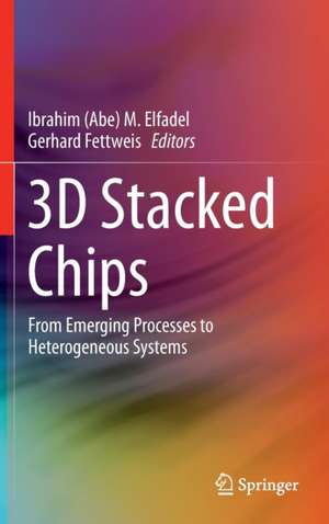
3D Stacked Chips: From Emerging Processes to Heterogeneous Systems
Editat de Ibrahim (Abe) M. Elfadel, Gerhard Fettweisen Limba Engleză Hardback – 23 mai 2016
| Toate formatele și edițiile | Preț | Express |
|---|---|---|
| Paperback (1) | 391.99 lei 6-8 săpt. | |
| Springer International Publishing – 26 mai 2018 | 391.99 lei 6-8 săpt. | |
| Hardback (1) | 399.50 lei 6-8 săpt. | |
| Springer International Publishing – 23 mai 2016 | 399.50 lei 6-8 săpt. |
Preț: 399.50 lei
Nou
Puncte Express: 599
Preț estimativ în valută:
76.44€ • 79.81$ • 63.27£
76.44€ • 79.81$ • 63.27£
Carte tipărită la comandă
Livrare economică 04-18 aprilie
Preluare comenzi: 021 569.72.76
Specificații
ISBN-13: 9783319204802
ISBN-10: 3319204807
Pagini: 300
Ilustrații: XXIII, 339 p. 238 illus., 157 illus. in color.
Dimensiuni: 155 x 235 x 26 mm
Greutate: 0.69 kg
Ediția:1st ed. 2016
Editura: Springer International Publishing
Colecția Springer
Locul publicării:Cham, Switzerland
ISBN-10: 3319204807
Pagini: 300
Ilustrații: XXIII, 339 p. 238 illus., 157 illus. in color.
Dimensiuni: 155 x 235 x 26 mm
Greutate: 0.69 kg
Ediția:1st ed. 2016
Editura: Springer International Publishing
Colecția Springer
Locul publicării:Cham, Switzerland
Public țintă
Professional/practitionerCuprins
Introduction to Electrical 3D Integration.- Copper-based TSV – Interposer.- Multi-TSV Crosstalk Channel Equalization with Non-Uniform Quantization.- Energy Efficient Electrical Intra-Chip Stack Communication.- Clock Generators for Heterogeneous MPSoCs within 3D Chip Stacks.- Energy Efficient Communications Employing 1-Bit Quantization at the Receiver.- 2-nm Laser Synthesized Si-Nanoparticles for Low Power Memory Applications.- Accurate Temperature Measurement for 3D Thermal Management.- EDA Environments for 3D Chip Stacks.- Integrating 3D Floorplanning and Optimization of Thermal Through-Silicon Vias.- Introduction to Optical Inter- and Intraconnects.- Optical Through-Silicon Vias.- Integrated Optical Devices for 3D Photonic Transceivers.- Cantilever Design for Tunable WDM Filters based on Silicon Microring Resonators.- Athermal photonic circuits for optical on-chip interconnects.- Integrated Circuits for 3D Photonic Transceivers.- Review of interdigitated back contacted full heterojunction solar cell (IBC-SHJ): a simulation approach.-
Recenzii
“The book is valuable as a learning tool for 3D stacked chips through TSVs … . a valuable addition to a scientific library, as well as served as good introduction for device reliability engineers or specialists and industrials involved in the field of 3D stacking in wafer fabrication and integrated circuit design. … highly recommended for people who desire a better understanding of the theory and practice of 3D TSVs and technical considerations in 3D chips floorplanning, modeling and characterization.” (Chong Leong Gan and Uda Hashim, Microelectronics Reliability, Vol. 63, August, 2016)
Notă biografică
Ibrahim (Abe) M. Elfadel has 15 years of industrial experience in the research, development and deployment of advanced computer-aided design (CAD) tools and methodologies for deep-submicron, high-performance digital designs. Most recently, he played a key role in the development and deployment of IBM’s next-generation layout verification tools for the ultra-deep submicron CMOS technology nodes. Dr. Elfadel is the recipient of six Invention Achievement Awards, an Outstanding Technical Achievement Award and a Research Division Award, all from IBM, for his contributions in the area of VLSI CAD. He is currently serving as an Associate Editor for the IEEE Transactions on Computer-Aided Design for Integrated Circuits and Systems.
Gerhard Fettweis earned his Ph.D. under H. Meyr's supervision from RWTH Aachen in 1990. After one year at IBM Research in San Jose, CA he moved to TCSI Inc., Berkeley, CA. Since 1994 he is Vodafone Chair Professor at TU Dresden, Germany, with currently 20 companies from Asia/Europe/US sponsoring his research on wireless transmission and chip design. He coordinates 2 DFG centers at TU Dresden, cfAED and HAEC. Gerhard is IEEE Fellow, member of acatech, has an honorary doctorate from TU Tampere, and has received multiple awards. In Dresden he has spun-out ten start-ups, and setup funded projects of more than EUR 1/3 billion volume. He has helped organized IEEE conferences, most notably as TPC Chair of IEEE ICC 2009, IEEE TTM 2012, and Ge
neral Chair of VTC Spring 2013. He remains active within IEEE.
Textul de pe ultima copertă
This book explains for readers how 3D chip stacks promise to increase the level of on-chip integration, and to design new heterogeneous semiconductor devices that combine chips of different integration technologies (incl. sensors) in a single package of the smallest possible size. The authors focus on heterogeneous 3D integration, addressing some of the most important challenges in this emerging technology, including contactless, optics-based, and carbon-nanotube-based 3D integration, as well as signal-integrity and thermal management issues in copper-based 3D integration. Coverage also includes the 3D heterogeneous integration of power sources, photonic devices, and non-volatile memories based on new materials systems.
•Provides single-source reference to the latest research in 3D optoelectronic integration: process, devices, and systems;
•Explains the use of wireless 3D integration to improve 3D IC reliability and yield;
•Describes techniques for monitoring and mitigating thermal behavior in 3D ICs;•Includes discussion of 3D integration of high-density power sources and novel NVM.
Caracteristici
Provides single-source reference to the latest research in 3D optoelectronic integration: process, devices, and systems; Explains the use of wireless 3D integration to improve 3D IC reliability and yield; Describes techniques for monitoring and mitigating thermal behavior in 3D ICs; Includes discussion of 3D integration of high-density power sources and novel NVM. Includes supplementary material: sn.pub/extras
