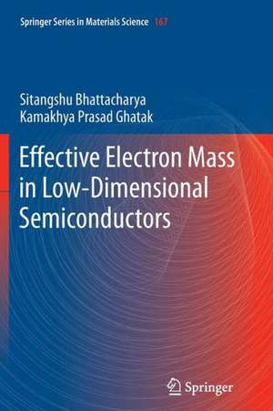
Effective Electron Mass in Low-Dimensional Semiconductors: Springer Series in Materials Science, cartea 167
Autor Sitangshu Bhattacharya, Kamakhya Prasad Ghataken Limba Engleză Paperback – 9 noi 2014
The book is written for post graduate students, researchers and engineers, professionals in the fields of solid state sciences, materials science, nanoscience and technology, nanostructured materials and condensed matter physics.
| Toate formatele și edițiile | Preț | Express |
|---|---|---|
| Paperback (1) | 956.99 lei 6-8 săpt. | |
| Springer Berlin, Heidelberg – 9 noi 2014 | 956.99 lei 6-8 săpt. | |
| Hardback (1) | 959.98 lei 6-8 săpt. | |
| Springer Berlin, Heidelberg – 6 oct 2012 | 959.98 lei 6-8 săpt. |
Din seria Springer Series in Materials Science
- 18%
 Preț: 1820.22 lei
 - 18%
 Preț: 776.09 lei
 - 24%
 Preț: 689.69 lei
 - 18%
 Preț: 968.96 lei
 - 20%
 Preț: 568.95 lei
 - 18%
 Preț: 953.65 lei
 - 18%
 Preț: 902.36 lei
 - 18%
 Preț: 953.65 lei
 - 20%
 Preț: 948.42 lei
 - 18%
 Preț: 1143.07 lei
 - 18%
 Preț: 1111.53 lei
 - 18%
 Preț: 1103.62 lei
 - 18%
 Preț: 1225.94 lei
 -
 Preț: 473.91 lei
 - 18%
 Preț: 782.42 lei
 -
 Preț: 433.47 lei
 - 18%
 Preț: 1116.40 lei
 - 18%
 Preț: 946.24 lei
 - 18%
 Preț: 945.20 lei
 - 18%
 Preț: 1114.21 lei
 - 15%
 Preț: 641.20 lei
 - 18%
 Preț: 958.56 lei
 - 18%
 Preț: 1224.36 lei
 - 15%
 Preț: 644.82 lei
 - 24%
 Preț: 833.45 lei
 - 24%
 Preț: 1060.36 lei
 - 18%
 Preț: 964.10 lei
 - 18%
 Preț: 1224.36 lei
 - 18%
 Preț: 1221.20 lei
 - 18%
 Preț: 946.87 lei
 - 18%
 Preț: 1836.92 lei
 - 15%
 Preț: 643.34 lei
 - 18%
 Preț: 1246.32 lei
 - 18%
 Preț: 956.81 lei
 - 18%
 Preț: 953.52 lei
 - 15%
 Preț: 637.59 lei
Preț: 956.99 lei
Preț vechi: 1167.06 lei
-18% Nou
Puncte Express: 1435
Preț estimativ în valută:
183.12€ • 199.54$ • 154.31£
183.12€ • 199.54$ • 154.31£
Carte tipărită la comandă
Livrare economică 23 aprilie-07 mai
Preluare comenzi: 021 569.72.76
Specificații
ISBN-13: 9783642438646
ISBN-10: 3642438644
Pagini: 560
Ilustrații: XXIV, 536 p.
Dimensiuni: 155 x 235 x 29 mm
Greutate: 0.78 kg
Ediția:2013
Editura: Springer Berlin, Heidelberg
Colecția Springer
Seria Springer Series in Materials Science
Locul publicării:Berlin, Heidelberg, Germany
ISBN-10: 3642438644
Pagini: 560
Ilustrații: XXIV, 536 p.
Dimensiuni: 155 x 235 x 29 mm
Greutate: 0.78 kg
Ediția:2013
Editura: Springer Berlin, Heidelberg
Colecția Springer
Seria Springer Series in Materials Science
Locul publicării:Berlin, Heidelberg, Germany
Public țintă
ResearchCuprins
Part I: Influence of Light Waves on the Effective Electron Mass (EEM) in Optoelectronic Semiconductors.- Part II: Influence of Quantum Confinement on the EEM in Non-Parabolic Semiconductors.- Part III: The EEM in Quantum Confined Superlattices of Non- Parabolic Semiconductors.- Part IV: Influence of Intense Electric Field on the EEM in Optoelectronic Semiconductors.
Notă biografică
Dr. S. Bhattacharya obtained his M. Sc. and Ph.D Degree from Electronic Science of the University of Calcutta and Jadavpur University, India in 2003 and 2009 respectively and is presently working at the Centre for Electronics Design and Technology, Indian Institute of Science, Bangalore. His current work involves the investigations of transport properties of different nanoscaled materials and devices under various external conditions. He is the co-author of more than 50 scientific research papers in different aspects of nanostructures in international peer-reviewed journals of high repute. He is also the co-author of the FOUR research monographs entitled "Einstein Relation in Compound Semiconductors and Their Nanostructures" Springer Series in Materials Science, Vol. 116,2009 which is the first book on Einstein relation and contains more than 100 open research problems, "Photoemission from Optoelectronic materials and their nanostructures",Springer Series in Nano structure Science and Technology, USA in 2009 as the first book solely devoted to Photoemission from nanostructured optoelectronic materials and contents more than 100 open research problems, "Thermo electric power in nano structured materials under strong magnetic field" Springer Series in Materials Science Vol. 137 ,2010 and contents one hundred and fifty open research problems and "Fowler-Nordheim Field Emission from Semiconductor Nanostructures" Springer Series in Solid State Sciences, Vol. 170, 2011 which is the first book on Fowler-Nordheim Field Emission containing 200 open research problems respectively. His present research interests are the quantum effect devices and nonlinearities. Besides, he is an invited speaker in different reputed International Conferences on nanoscale systems and devices.
Born in India in 1953.Professor K. P. Ghatak obtained his B.E degree in Electronics and Telecommunication Engineering in 1974 from the then Bengal Engineering college Shibpur(Presently Bengal Engineering and Science University) in 1974, M.Tech and PhD(Tech) degrees from the Institute of Radio Physics and Electronics of The University of Calcutta in 1976 and 1988 respectively.He joined as Lecturer in the Institute of Radio Physics and Electronics of the University of Calcutta in 1983, Reader in the Department of Electronics and Telecommunication of Jadavpur University in 1987 and Professor in the Department of Electronic Science of the University of Calcutta in 1994 and was at the top of the merit list in all the cases respectively. Professor K. P. Ghatak is the First Recipient of the Degree of Doctor of Engineering of Jadavpur University in 1991 since the University inception in 1955 and in the same year he received the Indian National Science Academy visiting fellowship to IIT-Kharagpur. His present research interests are nano science and number thoery. He is the principal co-author of more than 200 research papers on Semiconductor and Nanoscience in eminent peer-reviewed International Journals and more than 50 research papers in the Proceedings of the International Conferences held in USA and many of his papers are being cited many times. Professor Ghatak is the invited Speaker of SPIE, MRS, etc. and is the referee of different eminent Journals. He is the supervisor of more than two dozens of Ph.D candidates in various aspects of materials and nanoscience and many of them are working as Professor, Associate Professor and Assistant Professor in different Universities and reputed Academic Institutions. He is the principal co-author of the said FOUR research monographs. The All Indian Council For Technical Education has selected the first Research and Development project in his life for the best project award in Electronics and second best research project award considering all the branches of Engineering for the year 2006.
Born in India in 1953.Professor K. P. Ghatak obtained his B.E degree in Electronics and Telecommunication Engineering in 1974 from the then Bengal Engineering college Shibpur(Presently Bengal Engineering and Science University) in 1974, M.Tech and PhD(Tech) degrees from the Institute of Radio Physics and Electronics of The University of Calcutta in 1976 and 1988 respectively.He joined as Lecturer in the Institute of Radio Physics and Electronics of the University of Calcutta in 1983, Reader in the Department of Electronics and Telecommunication of Jadavpur University in 1987 and Professor in the Department of Electronic Science of the University of Calcutta in 1994 and was at the top of the merit list in all the cases respectively. Professor K. P. Ghatak is the First Recipient of the Degree of Doctor of Engineering of Jadavpur University in 1991 since the University inception in 1955 and in the same year he received the Indian National Science Academy visiting fellowship to IIT-Kharagpur. His present research interests are nano science and number thoery. He is the principal co-author of more than 200 research papers on Semiconductor and Nanoscience in eminent peer-reviewed International Journals and more than 50 research papers in the Proceedings of the International Conferences held in USA and many of his papers are being cited many times. Professor Ghatak is the invited Speaker of SPIE, MRS, etc. and is the referee of different eminent Journals. He is the supervisor of more than two dozens of Ph.D candidates in various aspects of materials and nanoscience and many of them are working as Professor, Associate Professor and Assistant Professor in different Universities and reputed Academic Institutions. He is the principal co-author of the said FOUR research monographs. The All Indian Council For Technical Education has selected the first Research and Development project in his life for the best project award in Electronics and second best research project award considering all the branches of Engineering for the year 2006.
Textul de pe ultima copertă
This book deals with the Effective Electron Mass (EEM) in low dimensional semiconductors. The materials considered are quantum confined non-linear optical, III-V, II-VI, GaP, Ge, PtSb2, zero-gap, stressed, Bismuth, carbon nanotubes, GaSb, IV-VI, Te, II-V, Bi2Te3, Sb, III-V, II-VI, IV-VI semiconductors and quantized III-V, II-VI, IV-VI and HgTe/CdTe superlattices with graded interfaces and effective mass superlattices. The presence of intense electric field and the light waves change the band structure of optoelectronic semiconductors in fundamental ways, which have also been incorporated in the study of the EEM in quantized structures of optoelectronic compounds that control the studies of the quantum effect devices under strong fields. The importance of measurement of band gap in optoelectronic materials under strong electric field and external photo excitation has also been discussed in this context. The influence of crossed electric and quantizing magnetic fields on the EEM and the EEM in heavily doped semiconductors and their nanostructures is discussed. This book contains 200 open research problems which form the integral part of the text and are useful for both Ph. D aspirants and researchers in the fields of solid-state sciences, materials science, nanoscience and technology and allied fields in addition to the graduate courses in modern semiconductor nanostructures.
The book is written for post graduate students, researchers and engineers, professionals in the fields of solid state sciences, materials science, nanoscience and technology, nanostructured materials and condensed matter physics.
The book is written for post graduate students, researchers and engineers, professionals in the fields of solid state sciences, materials science, nanoscience and technology, nanostructured materials and condensed matter physics.
Caracteristici
Provides a treatment of the effective electron mass in nanodevices Explains changes of the band structure of optoelectronic semiconductors by intense electric fields and light waves Gives insight into the electronic behavior in doped semiconductors and their nanostructures Supports tuition by 200 open problems and questions Includes supplementary material: sn.pub/extras
