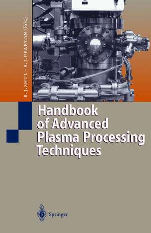
Handbook of Advanced Plasma Processing Techniques
Editat de R.J. Shul, S.J. Peartonen Limba Engleză Hardback – 28 aug 2000
| Toate formatele și edițiile | Preț | Express |
|---|---|---|
| Paperback (1) | 2100.36 lei 6-8 săpt. | |
| Springer Berlin, Heidelberg – noi 2012 | 2100.36 lei 6-8 săpt. | |
| Hardback (1) | 2104.78 lei 6-8 săpt. | |
| Springer Berlin, Heidelberg – 28 aug 2000 | 2104.78 lei 6-8 săpt. |
Preț: 2104.78 lei
Preț vechi: 2566.80 lei
-18% Nou
Puncte Express: 3157
Preț estimativ în valută:
402.73€ • 422.75$ • 334.29£
402.73€ • 422.75$ • 334.29£
Carte tipărită la comandă
Livrare economică 10-24 aprilie
Preluare comenzi: 021 569.72.76
Specificații
ISBN-13: 9783540667728
ISBN-10: 3540667725
Pagini: 672
Ilustrații: XVI, 655 p. 151 illus., 10 illus. in color.
Dimensiuni: 155 x 235 x 46 mm
Greutate: 1.05 kg
Ediția:2000
Editura: Springer Berlin, Heidelberg
Colecția Springer
Locul publicării:Berlin, Heidelberg, Germany
ISBN-10: 3540667725
Pagini: 672
Ilustrații: XVI, 655 p. 151 illus., 10 illus. in color.
Dimensiuni: 155 x 235 x 46 mm
Greutate: 1.05 kg
Ediția:2000
Editura: Springer Berlin, Heidelberg
Colecția Springer
Locul publicării:Berlin, Heidelberg, Germany
Public țintă
ResearchCuprins
1 Some Fundamental Aspects of Plasma-Assisted Etching.- 1.1 Introduction.- 1.2 The Evolution of Plasma Etching Equipment.- 1.3 The Role of Ions in Reactive Ion Etching.- 1.4 The Influence of the Reactor Walls and Other Surfaces.- 1.5 Ion Beam-Based Methods.- 1.6 Summary.- References.- 2 Plasma Fundamentals for Materials Processing.- 2.1 Introduction.- 2.2 Single Particle Motion.- 2.3 Collision Processes.- 2.4 Velocity Distributions.- 2.5 Sheaths.- 2.6 Plasma Transport.- 2.7 Dielectric Properties.- 2.8 Plasma Sources for Thin Films Processing.- References.- 3 Plasma Modeling.- 3.1 Introduction.- 3.2 Historical Perspective.- 3.3 Plasma Modeling Issues.- 3.4 Chemical Reaction Mechanisms.- 3.5 Examples of Application of Plasma Modeling to Design or Optimization.- 3.6 Future Directions of Plasma Modeling.- References.- 4 Plasma Reactor Modeling.- 4.1 Introduction.- 4.2 Reactor Scale Model.- 4.3 Feature Level Modeling.- 4.4 Database Needs.- 4.5 Concluding Remarks.- References.- 5 Overview of Plasma Diagnostic Techniques.- 5.1 Introduction.- 5.2 Plasma Electrical Characterization.- 5.3 Optical Diagnostic Techniques.- References.- 6 Mass Spectrometric Characterization of Plasma Etching Processes.- 6.1 Introduction.- 6.2 Application to Fundamental Studies.- 6.3 Application in Etch Processing Reactors.- 6.4 Summary and Future Directions.- References.- 7 Fundamentals of Plasma Process-Induced Charging and Damage.- 7.1 Introduction.- 7.2 The Origin of Pattern-Dependent Charging.- 7.3 The Notching Effect.- 7.4 Other Profile Effects Influenced by Charging.- 7.5 Gate Oxide Degradation.- 7.6 Charging Reduction Methodology.- 7.7 Concluding Remarks.- References.- 8 Surface Damage Induced by Dry Etching.- 8.1 Introduction.- 8.2 Surface Damage in Si.- 8.3 Surface Damage in III-V Semiconductors.- 8.4 Damage Removal.- 8.5 Summary.- References.- 9 Photomask Etching.- 9.1 Introduction.- 9.2 Optical Lithography.- 9.3 X-Ray Lithography.- 9.4 SCALPEL.- 9.5 EUVL.- 9.6 Ion Projection Lithography.- 9.7 IPL Mask Distortion Issues.- 9.8 Conclusion.- References.- 10 Bulk Si Micromachining for Integrated Microsystems and MEMS Processing.- 10.1 Introduction.- 10.2 Etch Technologies.- 10.3 ECR Results.- 10.4 DRIE Results.- 10.5 DRIE Applications.- 10.6 Conclusions.- References.- 11 Plasma Processing of III-V Materials.- 11.1 Introduction.- 11.2 Dry Etching Techniques.- 11.3 Masking Materials and Methods.- 11.4 Dry Etching Chemistries.- 11.5 Dry Etching of GaAs and Related Materials.- 11.6 Dry Etching of InP and Related Materials.- 11.7 Dry Etching of GaN and Related Materials.- 11.8 Selective Dry Etching of III-V Materials.- 11.9 Conclusion.- References.- 12 Ion Beam Etching of Compound Semiconductors.- 12.1 Introduction.- 12.2 Definitions.- 12.3 Ion Sources.- 12.4 Historic Development.- 12.5 Grid Design, Beam Uniformity, and Divergence.- 12.6 Brief Overview of Etching Kinetics and Chemistry.- 12.7 Surface Quality and Etch Masking.- 12.8 RIBE Etch Technology.- 12.9 CAIBE Etch Technology.- 12.10 Endpoint Detection.- 12.11 Damage.- References.- 13 Dry Etching of InP Vias.- 13.1 Introduction.- 13.2 Past Difficulties in Obtaining High Rate Etching for InP.- 13.3 High Density Plasma Sources for High InP Etch Rate.- 13.4 Measurement of Plasma Heating for InP Etching.- 13.5 Application to Via Hole Etching.- 13.6 Summary.- References.- 14 Device Damage During Low Temperature High-Density Plasma Chemical Vapor Deposition.- 14.1 Introduction.- 14.2 Experimental.- 14.3 Results and Discussion.- 14.4 Summary and Conclusions.- References.- 15 Dry Etching of Magnetic Materials.- 15.1Introduction.- 15.2 Ion Milling.- 15.3 Cl2-Based ICP Etching of NiFe and Related Materials.- 15.4 Copper Dry Etching in Cl2/Ar.- 15.5 CO/NH3 Etching of Magnetic Materials.- 15.6 ECR and ICP Etching of NiMnSb.- 15.7 Dry Etching of LaCaMnOx and SmCo.- 15.8 Summary and Conclusions.- References.
Textul de pe ultima copertă
This volume covers the topic of advanced plasma processing techniques, from the fundamental physics of plasmas to diagnostics, modeling and applications such as etching and deposition for microelectronics. The use of plasmas for patterning on a submicron scale has enabled successive generations of continually smaller transistors, lasers, micromachines, sensors and magnetic read/write heads that have formed the basis of our information age. This volume is the first to give coverage to this broad area of topics in a detailed fashion, especially in the rapidly expanding fields of micro-mechanical machines, photomask fabrication, magnetic data storage and reactor modeling. It provides the reader with a broad array of topics, authored by the leading experts in the field.
Caracteristici
This volume brings together some of the most well-known scientists in each of the topics covered, many of whom have pioneered the development of plasma processing techniques Includes supplementary material: sn.pub/extras
