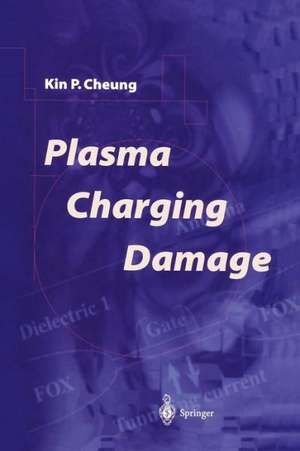
Plasma Charging Damage
Autor Kin P. Cheungen Limba Engleză Paperback – 30 aug 2012
| Toate formatele și edițiile | Preț | Express |
|---|---|---|
| Paperback (1) | 1219.94 lei 6-8 săpt. | |
| SPRINGER LONDON – 30 aug 2012 | 1219.94 lei 6-8 săpt. | |
| Hardback (1) | 1225.16 lei 6-8 săpt. | |
| SPRINGER LONDON – 4 oct 2000 | 1225.16 lei 6-8 săpt. |
Preț: 1219.94 lei
Preț vechi: 1487.73 lei
-18% Nou
Puncte Express: 1830
Preț estimativ în valută:
233.43€ • 254.36$ • 196.70£
233.43€ • 254.36$ • 196.70£
Carte tipărită la comandă
Livrare economică 23 aprilie-07 mai
Preluare comenzi: 021 569.72.76
Specificații
ISBN-13: 9781447110620
ISBN-10: 1447110625
Pagini: 364
Ilustrații: XII, 346 p.
Dimensiuni: 155 x 235 x 19 mm
Greutate: 0.51 kg
Ediția:Softcover reprint of the original 1st ed. 2001
Editura: SPRINGER LONDON
Colecția Springer
Locul publicării:London, United Kingdom
ISBN-10: 1447110625
Pagini: 364
Ilustrații: XII, 346 p.
Dimensiuni: 155 x 235 x 19 mm
Greutate: 0.51 kg
Ediția:Softcover reprint of the original 1st ed. 2001
Editura: SPRINGER LONDON
Colecția Springer
Locul publicării:London, United Kingdom
Public țintă
Professional/practitionerCuprins
1. Thin Gate-oxide Wear-out and Breakdown.- 1.1 The MOSFET.- 1.2 Tunneling Phenomena in Thin Oxide.- 1.3 Thin Oxide Breakdown Measurements.- 1.4 Gate-oxide Breakdown Models.- 1.5 Trap Generation Model and Acceleration Factors.- 1.6 Defects, Traps and Latent Defects.- References.- 2. Mechanism of Plasma Charging Damage I.- 2.1 Basic Plasma Characteristics.- 2.2 Charge Balance and Plasma Charging.- 2.3 Charging in the Presence of an Applied Bias.- 2.4 Fowler-Nordheim (FN) Tunneling and Charge Balance.- 2.5 Antenna Effect.- 2.6 Uniformity of Electron Temperature.- 2.7 Charging Damage by High-density Plasma.- References.- 3. Mechanism of Plasma Charging Damage II.- 3.1 Electron-shading Effect.- 3.2 AC Charging Effect.- 3.3 RF Bias Transient Charging Damage.- References.- 4. Mechanism of Plasma Charging Damage III.- 4.1 Plasma Charging Damage from Dielectric Deposition.- 4.2 Plasma Charging Damage from Magnetized Plasma.- 4.3 Plasma Charging Damage at the Transistor Channel’s Edge.- 4.4 Plasma Charging Damage in Very Short Range.- 4.5 Hidden Antenna Effects.- References.- 5. Charging Damage Measurement I ¡ª Determination of Plasma’s Ability to Cause Damage.- 5.1 Direct Plasma Property Measurement with Langmuir Probe.- 5.2 Stanford Plasma-On-Wafer Real-Time (SPORT) Probe.- 5.3 Using MNOS Device to Measure Plasma Charging Voltage.- 5.4 EEPROM and CHARM®.- 5.5 Common Problems with Methods that Measure Plasma Properties Directly.- 5.6 Rapid In-line Charge Sensing Methods.- References.- 6. Charging Damage Measurement II ¡ª Direct Measurement of Damage.- 6.1 Measurement Challenge.- 6.2 Test Devices.- 6.3 Breakdown Tests.- 6.4 Wear-out Tests.- References.- 7. Coping with Plasma Charging Damage.- 7.1 Impact of Plasma Charging Damage on Yield and Reliability.- 7.2 Fixing theDamaging Process.- 7.3 Use of Design Rules.- 7.4 Diode Protection.- 7.5 Failure Criteria Problem.- 7.6 Projecting the Yield Impact to Products.- 7.7 Projecting the Reliability Impact to Products.- 7.8 Ultra-thin Gate-oxide Issues.- 7.9 The Damage Measurement Problem for Ultra-thin Gate-oxide.- References.
Caracteristici
The only book of its kind - the only competition on subject matter comes from a Japanese language text to which this author is also a contributor It is neither as coherent nor as comprehensive as the current text The books readership runs the whole gamut of experience in the subject The author works at AT&T's Bell Laboratories in New Jersey This laboratory is a world leader in many areas of technology
