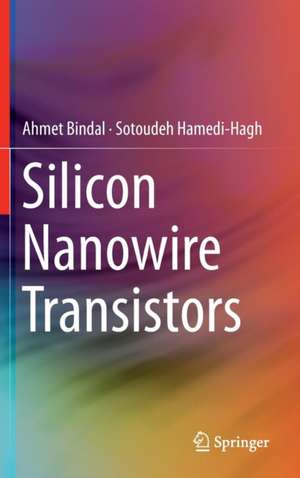
Silicon Nanowire Transistors
Autor Ahmet Bindal, Sotoudeh Hamedi-Haghen Limba Engleză Hardback – 2 mar 2016
| Toate formatele și edițiile | Preț | Express |
|---|---|---|
| Paperback (1) | 572.65 lei 43-57 zile | |
| Springer International Publishing – 7 apr 2018 | 572.65 lei 43-57 zile | |
| Hardback (1) | 578.84 lei 43-57 zile | |
| Springer International Publishing – 2 mar 2016 | 578.84 lei 43-57 zile |
Preț: 578.84 lei
Preț vechi: 680.99 lei
-15% Nou
Puncte Express: 868
Preț estimativ în valută:
110.76€ • 115.94$ • 92.19£
110.76€ • 115.94$ • 92.19£
Carte tipărită la comandă
Livrare economică 31 martie-14 aprilie
Preluare comenzi: 021 569.72.76
Specificații
ISBN-13: 9783319271750
ISBN-10: 331927175X
Pagini: 200
Ilustrații: XIV, 165 p. 145 illus., 5 illus. in color.
Dimensiuni: 155 x 235 x 11 mm
Greutate: 0.43 kg
Ediția:1st ed. 2016
Editura: Springer International Publishing
Colecția Springer
Locul publicării:Cham, Switzerland
ISBN-10: 331927175X
Pagini: 200
Ilustrații: XIV, 165 p. 145 illus., 5 illus. in color.
Dimensiuni: 155 x 235 x 11 mm
Greutate: 0.43 kg
Ediția:1st ed. 2016
Editura: Springer International Publishing
Colecția Springer
Locul publicării:Cham, Switzerland
Public țintă
ResearchCuprins
Dual Work Function Silicon Nanowire MOS Transistors.- Single Work Function Silicon Nanowire MOS Transistors.- Spice Modeling For Analog and Digital Applications.- High-Speed Analog Applications.- Radio Frequency (RF) Applications.- SRAM Mega Cell Design for Digital Applications.- Field-Programmable-Gate-Array (FPGA).- Integrate-And-Fire Spiking (IFS) Neuron.- Direct Sequence Spread Spectrum (DSSS) Base-Band Transmitter.-
Notă biografică
Ahmet Bindal received his M.S. and Ph.D. degrees inElectrical Engineering Department from the University of California, LosAngeles CA. His doctoral research was the material characterization andanalysis of HEMT GaAs transistors. During his graduate studies, he was aresearch associate and technical consultant for Hughes Aircraft Co. In 1988, hejoined the technical staff of IBM Research and Development Center in Fishkill,NY, where he worked as a device design and characterization engineer. Hedeveloped asymmetrical MOS transistors and ultra thin Silicon-On-Insulator (SOI)technologies for IBM. In 1993, he transferred to IBM in Rochester, MN, as asenior circuit design engineer to work on the floating-point unit for AS-400main frame processor. He continued his circuit design career at IntelCorporation in Santa Clara, CA, where he designed 16-bit packed multipliers andadders for the MMX unit for Pentium II processors. In 1996, he joined PhilipsSemiconductors in Sunnyvale, CA, where he was involved in the designs ofinstruction and data caches, and various SRAM modules for the Trimediaprocessor. His involvement with VLSI architecture also started in PhilipsSemiconductors and led to the design of the Video-Out unit for the sameprocessor. In 1998, he joined Cadence Design Systems as a VLSI architect anddirected a team of engineers to design self-timed asynchronous processors.After approximately 20 years of industry work, he joined the ComputerEngineering faculty at San Jose State University in 2002. His current researchinterests range from nano-scale electron devices to nano-scale architecturesand robotics. Dr. Bindal has over 30 refereed scientific publications and 10invention disclosures with IBM. He currently holds three U.S. patents with IBMand one with Intel Corporation.
Dr. Hamedi-Hagh received his Ph.D. from the Universityof Toronto, Canada in 2004. He joined the Electrical Engineering Department atSan Jose State University (SJSU) in 2005. His areas of research and expertise includehigh frequency modeling of semiconductor device structures and design of RadioFrequency, Analog and Mixed-Signal integrated circuits for wireless andwireline communication systems. Dr. Hamedi-Hagh has developed the Radio FrequencyIntegrated Circuits laboratory and curriculum at both graduate and undergraduatelevels with over $0.5M research funding and through close collaborations with industries.He has received several California State University (CSU) professional developmentgrants, CSU Research Funds, Research, Scholarship and Creative Activity (RSCA)grants, SJSU Planning Council Grants, College of Engineering professionaldevelopment grants and Junior Faculty Career Development Grants. He is afounding member of SJSU Smart Technology and Computing Center for ComplexSystems (STCCS). In 2016, he was appointed as the Mixed-Signal endowed chair ofthe Electrical Engineering department. Dr. Hamedi-Hagh has over 30 refereedscientific journal and conference paper publications in prestigious nationaland international Institutes and societies. He received the best paper award atthe Micronet Symposium in Quebec, Canada in 2001 and the IEEE InternationalSymposium on Personal, Indoor and Mobile Radio Communications in Barcelona,Spain in 2004. Dr. Hamedi-Hagh has advised several hundred projects on designof integrated circuits and systems. He holds seven US and world patents on wirelesscircuits, systems and cryptography. His latest patent introduces suspendance®and trajectance® laws as alternatives to Kirchhoff’s laws forcircuit analysis.
Textul de pe ultima copertă
This book describes the n and p-channel Silicon Nanowire Transistor (SNT) designs with single and dual-work functions, emphasizing low static and dynamic power consumption. The authors describe a process flow for fabrication and generate SPICE models for building various digital and analog circuits. These include an SRAM, a baseband spread spectrum transmitter, a neuron cell and a Field Programmable Gate Array (FPGA) platform in the digital domain, as well as high bandwidth single-stage and operational amplifiers, RF communication circuits in the analog domain, in order to show this technology’s true potential for the next generation VLSI.
- Describes Silicon Nanowire (SNW) Transistors, as vertically constructed MOS n and p-channel transistors, with low static and dynamic power consumption and small layout footprint;
- Targets System-on-Chip (SoC) design, supporting very high transistor count (ULSI), minimal powerconsumption requiring inexpensive substrates for packaging;
- Enables fabrication of different types of memory on the same chip, such as capacitive cells and transistors with floating gates that can be used as DRAMs and Flash memories.
Caracteristici
Describes Silicon Nanowire (SNW) Transistors, as vertically constructed MOS n and p-channel transistors, with low static and dynamic power consumption and small layout footprint; Targets System-on-Chip (SoC) design, supporting very high transistor count (ULSI), minimal power consumption requiring inexpensive substrates for packaging; Enables fabrication of different types of memory on the same chip, such as capacitive cells and transistors with floating gates that can be used as DRAMs and Flash memories. Includes supplementary material: sn.pub/extras


