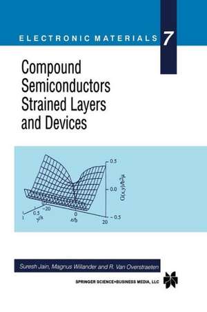
Compound Semiconductors Strained Layers and Devices: Electronic Materials Series, cartea 7
Editat de Suresh Jain, Magnus Willander, R. Van Overstraetenen Limba Engleză Paperback – 14 mar 2014
| Toate formatele și edițiile | Preț | Express |
|---|---|---|
| Paperback (1) | 947.18 lei 6-8 săpt. | |
| Springer Us – 14 mar 2014 | 947.18 lei 6-8 săpt. | |
| Hardback (1) | 953.20 lei 6-8 săpt. | |
| Springer Us – 31 mar 2000 | 953.20 lei 6-8 săpt. |
Preț: 947.18 lei
Preț vechi: 1155.11 lei
-18% Nou
Puncte Express: 1421
Preț estimativ în valută:
181.26€ • 196.83$ • 152.26£
181.26€ • 196.83$ • 152.26£
Carte tipărită la comandă
Livrare economică 22 aprilie-06 mai
Preluare comenzi: 021 569.72.76
Specificații
ISBN-13: 9781461370000
ISBN-10: 1461370000
Pagini: 352
Ilustrații: XII, 337 p. 8 illus.
Dimensiuni: 155 x 235 x 18 mm
Greutate: 0.49 kg
Ediția:2000
Editura: Springer Us
Colecția Springer
Seria Electronic Materials Series
Locul publicării:New York, NY, United States
ISBN-10: 1461370000
Pagini: 352
Ilustrații: XII, 337 p. 8 illus.
Dimensiuni: 155 x 235 x 18 mm
Greutate: 0.49 kg
Ediția:2000
Editura: Springer Us
Colecția Springer
Seria Electronic Materials Series
Locul publicării:New York, NY, United States
V-ar putea interesa
-
 Superconductivity, Superfluids and CondensatesJames F. Annett-10%Preț: 274.60 lei303.94 lei
 -
 -11%Preț: 339.69 lei382.26 lei
 -
 SuperconductorsA. V. Narlikar-30%Preț: 654.94 lei929.64 lei
 -
 MicrocavitiesAlexey Kavokin-18%Preț: 383.64 lei466.49 lei
 -
 -9%Preț: 771.10 lei847.36 lei
 -
 Preț: 471.75 lei
 -
 -23%Preț: 1031.28 lei1339.33 lei
 -
 -9%Preț: 1249.95 lei1373.58 lei
 -
 -18%Preț: 1561.41 lei1904.16 lei
 -
 Silicon Carbide Radiation DetectorsMarzio De Napoli-27%Preț: 476.87 lei650.33 lei
Public țintă
ResearchCuprins
1 Introduction.- 1.1 Evolution of strained layers.- 1.2 Conventional III-V-based heterostructures.- 1.3 III-Nitrides.- 1.4 Wide bandgap II-VI semiconductors.- 1.5 Material parameters.- 1.6 Scope and organization of this book.- 2 Characterization and growth.- 2.1 Methods of characterization.- 2.2 Epitaxial growth methods.- 2.3 Growth of conventional III-V semiconductors.- 2.4 Growth of II-VI semiconductors.- 2.5 Growth of Ill-nitride epilayers.- 3 Strain and critical thickness.- 3.1 Strain and energies of epilayers.- 3.2 Processes involved in dislocation generation.- 3.3 Critical thickness.- 4 Strain relaxation and defects.- 4.1 Strain in GeSi layers.- 4.2 Strain in III-V semiconductor layers.- 4.3 Strain in II-VI layers.- 4.4 Strain and defects in Ill-Nitride layers.- 5 Band structure and optical properties.- 5.1 Band structure.- 5.2 Band offsets.- 5.3 Optical properties of III-V semiconductors.- 5.4 Optical properties of II-VI semiconductors.- 5.5 Optical properties of Ill-Nitrides.- 6 Electrical and magnetic properties.- 6.1 Electrical properties of II-VI semiconductors.- 6.2 Electrical properties of n-type GaN.- 6.3 Electrical properties of p-type Ill-Nitrides.- 6.4 Electrical properties A1N, InN and alloys.- 6.5 Schottky barriers and ohmic contacts.- 6.6 Effect of applied electric field.- 6.7 Piezoelectric effect.- 6.8 Effect of magnetic field on semiconductors.- 7 Strained layer optoelectronic devices.- 7.1 Conventional-Ill-V semiconductor lasers.- 7.2 ZnSe-based light emitters and other devices.- 7.3 Other II-VI semiconductor applications.- 7.4 Ill-Nitride Light Emitting Diodes.- 7.5 GaN based Lasers.- 8 Transistors.- 8.1 InGaAs transistors.- 8.2 II-VI semiconductor transistors.- 8.3 Ill-Nitride based transistors.- 8.4 Device Processing.- 9 Summary and conclusions.- 9.1 Growth, defects and strain.- 9.2 Band structure and electronic properties.- 9.3 Applications and future work.- Appendix A.