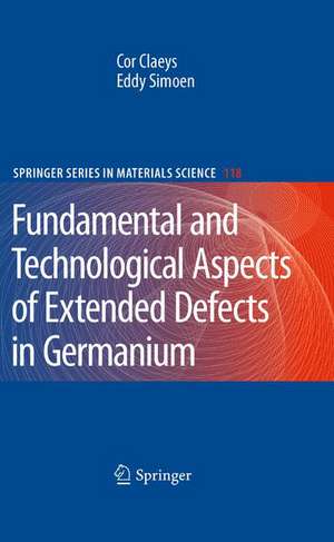
Extended Defects in Germanium: Fundamental and Technological Aspects: Springer Series in Materials Science, cartea 118
Autor Cor Claeys, Eddy Simoenen Limba Engleză Hardback – 18 feb 2009
| Toate formatele și edițiile | Preț | Express |
|---|---|---|
| Paperback (1) | 786.77 lei 38-45 zile | |
| Springer Berlin, Heidelberg – 30 noi 2010 | 786.77 lei 38-45 zile | |
| Hardback (1) | 954.45 lei 6-8 săpt. | |
| Springer Berlin, Heidelberg – 18 feb 2009 | 954.45 lei 6-8 săpt. |
Din seria Springer Series in Materials Science
- 18%
 Preț: 1820.22 lei
 - 18%
 Preț: 776.09 lei
 - 24%
 Preț: 689.68 lei
 - 18%
 Preț: 968.96 lei
 - 20%
 Preț: 568.94 lei
 - 18%
 Preț: 953.65 lei
 - 18%
 Preț: 902.36 lei
 - 18%
 Preț: 953.65 lei
 - 20%
 Preț: 948.41 lei
 - 18%
 Preț: 1143.07 lei
 - 18%
 Preț: 1111.53 lei
 - 18%
 Preț: 1103.62 lei
 - 18%
 Preț: 1225.94 lei
 -
 Preț: 473.91 lei
 - 18%
 Preț: 782.42 lei
 -
 Preț: 433.47 lei
 - 18%
 Preț: 1116.40 lei
 - 18%
 Preț: 946.24 lei
 - 18%
 Preț: 945.20 lei
 - 15%
 Preț: 641.20 lei
 - 18%
 Preț: 958.56 lei
 - 18%
 Preț: 1224.36 lei
 - 15%
 Preț: 644.82 lei
 - 24%
 Preț: 833.43 lei
 - 24%
 Preț: 1060.33 lei
 - 18%
 Preț: 964.10 lei
 - 18%
 Preț: 1224.36 lei
 - 18%
 Preț: 1221.20 lei
 - 18%
 Preț: 946.87 lei
 - 18%
 Preț: 1842.31 lei
 - 15%
 Preț: 643.34 lei
 - 18%
 Preț: 1246.32 lei
 - 18%
 Preț: 956.81 lei
 - 18%
 Preț: 953.52 lei
 - 15%
 Preț: 637.59 lei
 - 24%
 Preț: 1060.87 lei
Preț: 954.45 lei
Preț vechi: 1163.97 lei
-18% Nou
Puncte Express: 1432
Preț estimativ în valută:
182.66€ • 189.25$ • 152.44£
182.66€ • 189.25$ • 152.44£
Carte tipărită la comandă
Livrare economică 21 martie-04 aprilie
Preluare comenzi: 021 569.72.76
Specificații
ISBN-13: 9783540856115
ISBN-10: 3540856110
Pagini: 345
Ilustrații: XX, 300 p.
Dimensiuni: 155 x 235 x 24 mm
Greutate: 0.7 kg
Ediția:2009
Editura: Springer Berlin, Heidelberg
Colecția Springer
Seria Springer Series in Materials Science
Locul publicării:Berlin, Heidelberg, Germany
ISBN-10: 3540856110
Pagini: 345
Ilustrații: XX, 300 p.
Dimensiuni: 155 x 235 x 24 mm
Greutate: 0.7 kg
Ediția:2009
Editura: Springer Berlin, Heidelberg
Colecția Springer
Seria Springer Series in Materials Science
Locul publicării:Berlin, Heidelberg, Germany
Public țintă
Professional/practitionerCuprins
Dislocations in Germanium: Mechanical Properties.- Electrical and Optical Properties.- Grain Boundaries in Germanium.- Germanium-Based Substrate Defects.- Process-Induced Defects in Germanium.
Notă biografică
Cor Claeys was born in Antwerp, Belgium. He received the electrical-mechanical engineering degree in 1974 and the Ph.D. degree in 1979, both from the Katholieke Universiteit Leuven (KU Leuven), Belgium. From 1974 to 1984 he was a Research Assistant and Staff Member, respectively, of the ESAT Laboratory of the KU Leuven and since 1990, a Professor. In 1984, he joined IMEC as Head of Silicon Processing Group. Since 1990 he was Head of the research group on Radiation Effects, Cryogenic Electronics and Noise Studies. Recently, he became responsible for Strategic Relations and is for IMEC on the management board of several projects funded by the European Commission (NANOCMOS, SINANO, FLYING WAFER, CADRES, STAR, EUROSOI, SEA-NET, PULLNANO…). He is also member of the European Expert Group on Nanosciences. His main interests are in general silicon technology for ULSI, device physics, including low-temperature operation, low frequency noise phenomena and radiation effects, and defect engineering and material characterization. He coedited a book "Low Temperature Electronics" and on "Germanium-Based Technologies: From Materials to Devices" and wrote a monograph on "Radiation Effects in Advanced Semiconductor Materials and Devices". He also authored and co-authored eight book chapters and more than 700 technical papers and conference contributions related to the above fields. He has been involved in the organisation of a large number of international conferences and edited more than 35 Proceedings Volumes. He is an associated Editor for the Journal of the Electrochemical Society. He had short stays as Visiting Professor at the Queens University in Belfast, Ireland, and the University of Calabria, Italy. Prof. Claeys is a member of the European Material Research Society, a Senior Member of IEEE and a Fellow of the Electrochemical Society. He was the founder of the IEEE Electron Devices Benelux Chapter, was Chair of the IEEE Benelux Section, was in the period 1999-2005elected AdCom member of the Electron Devices Society (EDS), and was EDS Vice-President for Chapters and Regions during 2000-2006. Since 2000 he is an EDS Distinguished Lecture. In 2006, he has been elected as EDS President-Elect. He also received the IEEE Third Millennium Medal. Within the Electrochemical Society he has been serving in different committees and was Chair of the Electronics Division (2001-2003). In 1999 he was elected as Academician and Professor of the International Information Academy. In 2004 he received the Electronics Division Award of the Electrochemical Society.
Eddy Simoen obtained his Masters ('80) and Doctoral Degree ('85) in Engineering from the University of Gent (Belgium). His doctoral thesis was devoted to the study of trap levels in high-purity germanium by deep-level transient spectroscopy. In 1986, he joined IMEC to work in the field of low temperature electronics. His current interests cover the field of device physics and defect engineering in general, with particular emphasis on the study of low-frequency noise, low-temperature behavior and of radiation defects in semiconductor components and materials. He is an IMEC Scientist, currently involved in the study of defect and strain engineering in high-mobility and epitaxial substrates and defect studies in germanium. In these fields, he has (co-) authored over 900 Journal and Conference papers and in addition 11 book chapters and a monograph on Radiation Effects in Advanced Semiconductor Devices and Materials (Springer, 2002) whereof the Chinese translation will appear in December 2007. He was also a co-editor of the book on Germanium-based Technologies - from Materials to Devices (Elsevier March 2007). He acted as co-editor of four International Conference Proceedings and was a lecturer at the International Noise School held at IMEC in 1993, at the ENDEASD Workshop in Santorini (Greece; april 1999) and Stockholm (Sweden, June 2000) and at the EUROSOI Workshop in Leuven (January, 2007).
Eddy Simoen obtained his Masters ('80) and Doctoral Degree ('85) in Engineering from the University of Gent (Belgium). His doctoral thesis was devoted to the study of trap levels in high-purity germanium by deep-level transient spectroscopy. In 1986, he joined IMEC to work in the field of low temperature electronics. His current interests cover the field of device physics and defect engineering in general, with particular emphasis on the study of low-frequency noise, low-temperature behavior and of radiation defects in semiconductor components and materials. He is an IMEC Scientist, currently involved in the study of defect and strain engineering in high-mobility and epitaxial substrates and defect studies in germanium. In these fields, he has (co-) authored over 900 Journal and Conference papers and in addition 11 book chapters and a monograph on Radiation Effects in Advanced Semiconductor Devices and Materials (Springer, 2002) whereof the Chinese translation will appear in December 2007. He was also a co-editor of the book on Germanium-based Technologies - from Materials to Devices (Elsevier March 2007). He acted as co-editor of four International Conference Proceedings and was a lecturer at the International Noise School held at IMEC in 1993, at the ENDEASD Workshop in Santorini (Greece; april 1999) and Stockholm (Sweden, June 2000) and at the EUROSOI Workshop in Leuven (January, 2007).
Textul de pe ultima copertă
The aim is to give an overview of the physics of extended defects in Germanium, i.e. dislocations (line defects), grain boundaries, stacking faults, twins and {311} defects (two-dimensional defects) and precipitates, bubbles, etc. The first part covers fundamentals, describing the crystallographic structure and other physical and electrical properties, mainly of dislocations. Since dislocations are essential for the plastic deformation of Germanium, methods for analysis and imaging of dislocations and to evaluate their structure are described. Attention is given to the electrical and optical properties, which are important for devices made in dislocated Ge. The second part treats the creation of extended defects during wafer and device processing. Issues are addressed such as defect formation during ion implantation, necessary to create junctions, which are an essential part in every device type. Extended defects are also created during the deposition of thin or thick epitaxial layers on other substrates, which are important for optoelectronic and photovoltaic applications. In brief, the book is intended to provide a fundamental understanding of the extended-defect formation during Ge materials and device processing, providing ways to distinguish harmful from less detrimental defects and should point out ways for defect engineering and control.
Caracteristici
Deals with all aspects of defects in Ge, an element which is gaining importance again in semiconductor technology Discusses all kinds of expanded defects in Ge, such as dislocation, stacking faults, twins, grain boundaries and bubbles on a crystallographic basis Systematically presentation of defects creation and its influence on device properties Appeals mainly to researchers and engineers but is also suitable for graduate students working in this field Includes supplementary material: sn.pub/extras
