Offset Reduction Techniques in High-Speed Analog-to-Digital Converters: Analysis, Design and Tradeoffs: Analog Circuits and Signal Processing
Autor Pedro M. Figueiredo, João C. Vitalen Limba Engleză Paperback – 28 oct 2010
| Toate formatele și edițiile | Preț | Express |
|---|---|---|
| Paperback (1) | 1112.92 lei 6-8 săpt. | |
| SPRINGER NETHERLANDS – 28 oct 2010 | 1112.92 lei 6-8 săpt. | |
| Hardback (1) | 1119.08 lei 6-8 săpt. | |
| SPRINGER NETHERLANDS – 9 mar 2009 | 1119.08 lei 6-8 săpt. |
Din seria Analog Circuits and Signal Processing
- 5%
 Preț: 902.97 lei
 - 9%
 Preț: 629.00 lei
 -
 Preț: 388.34 lei
 - 15%
 Preț: 636.30 lei
 - 15%
 Preț: 636.80 lei
 - 18%
 Preț: 941.82 lei
 - 15%
 Preț: 639.08 lei
 - 18%
 Preț: 918.48 lei
 - 15%
 Preț: 631.21 lei
 - 15%
 Preț: 642.03 lei
 - 15%
 Preț: 641.85 lei
 - 18%
 Preț: 887.05 lei
 - 18%
 Preț: 944.51 lei
 - 15%
 Preț: 632.55 lei
 - 15%
 Preț: 641.03 lei
 - 18%
 Preț: 836.39 lei
 - 15%
 Preț: 642.18 lei
 - 15%
 Preț: 639.90 lei
 - 18%
 Preț: 947.85 lei
 - 15%
 Preț: 642.51 lei
 - 15%
 Preț: 631.86 lei
 - 15%
 Preț: 634.49 lei
 - 15%
 Preț: 635.47 lei
 - 15%
 Preț: 640.06 lei
 - 15%
 Preț: 631.53 lei
 - 15%
 Preț: 635.65 lei
 - 18%
 Preț: 941.50 lei
 - 15%
 Preț: 636.30 lei
 - 15%
 Preț: 633.19 lei
 - 15%
 Preț: 635.80 lei
 - 18%
 Preț: 888.01 lei
 - 18%
 Preț: 942.76 lei
 - 18%
 Preț: 1387.10 lei
 - 18%
 Preț: 1115.28 lei
 - 15%
 Preț: 633.68 lei
 - 15%
 Preț: 641.03 lei
 - 15%
 Preț: 638.57 lei
 - 15%
 Preț: 642.51 lei
 - 18%
 Preț: 947.85 lei
 - 15%
 Preț: 640.71 lei
 - 15%
 Preț: 640.88 lei
 - 15%
 Preț: 631.40 lei
 - 18%
 Preț: 944.19 lei
 - 18%
 Preț: 944.67 lei
 - 18%
 Preț: 942.94 lei
 - 15%
 Preț: 641.20 lei
 - 20%
 Preț: 555.53 lei
 - 18%
 Preț: 1003.38 lei
Preț: 1112.92 lei
Preț vechi: 1357.21 lei
-18% Nou
Puncte Express: 1669
Preț estimativ în valută:
212.99€ • 221.54$ • 175.83£
212.99€ • 221.54$ • 175.83£
Carte tipărită la comandă
Livrare economică 14-28 aprilie
Preluare comenzi: 021 569.72.76
Specificații
ISBN-13: 9789048181926
ISBN-10: 9048181925
Pagini: 404
Ilustrații: XX, 382 p.
Dimensiuni: 155 x 235 x 21 mm
Greutate: 0.56 kg
Ediția:Softcover reprint of hardcover 1st ed. 2009
Editura: SPRINGER NETHERLANDS
Colecția Springer
Seria Analog Circuits and Signal Processing
Locul publicării:Dordrecht, Netherlands
ISBN-10: 9048181925
Pagini: 404
Ilustrații: XX, 382 p.
Dimensiuni: 155 x 235 x 21 mm
Greutate: 0.56 kg
Ediția:Softcover reprint of hardcover 1st ed. 2009
Editura: SPRINGER NETHERLANDS
Colecția Springer
Seria Analog Circuits and Signal Processing
Locul publicării:Dordrecht, Netherlands
Public țintă
ResearchCuprins
Preface. List of Symbols and Abbreviations. 1 High-Speed ADC Architectures. 2 Averaging Technique - DC Analysis and Termination. 3 Averaging Technique - Transient Analysis and Automated Design. 4 Integrated Prototypes Using Averaging. 5 Offset Cancellation Methods. 6 Conclusions. Appendix A: Averaging With Piecewise Linear Differential Pairs. Appendix B: Mismatches In The Resistors Of The Aveaging Network. Appendix C Averaging In Folding Stages. References. Index.
Notă biografică
Pedro Figueiredo received the degrees of Licenciado and Doutor (PhD) in Electrical and Computer Engineering in 1999 and 2006, respectively, from the Instituto Superior Técnico (IST), Lisbon, Portugal. From 1997 to 1999, he was with the Analog and Mixed-Mode Circuits Group in the Institute for Systems and Computer Engineering (INESC), Lisbon, Portugal, where he worked on low-noise logic families and high-speed Analog-to-Digital Converters.
In 1999, he joined Chipidea - Microelectrónica, where he currently leads the group responsible for the design of Analog-to-Digital Converters. His main research interests are in the area of analog and mixed-signal circuits, with emphasis on high-speed data conversion and design automation. He has 10 publications in international journals and conferences.
João Vital received the degrees of Licenciado, Mestre and Doutor (PhD) in Electrical and Computer Engineering in 1986, 1990 and 1994, respectively, all from the Instituto Superior Técnico (IST), Lisboa, Portugal. He is a Co-founder of Chipidea - Microelectronica in 1997, and currently serves as Vice-President of Data Conversion, leading the Data Conversion Solutions Division of Chipidea to provide competitive solutions towards the demanding markets of Broadband Wireless Communications and Video. His main scientific interests are in the area of analog and mixed-signal integrated-circuit design, with a focus on data conversion. He developed research work in the University of Pavia, Italy, in the University of California - Los Angeles, USA, and in the Oregon State University, USA, also in 1990. He has over 50 publications in international journals, book chapters and conferences and is a co-holder of an European and US Patent filed by British Telecom.
Textul de pe ultima copertă
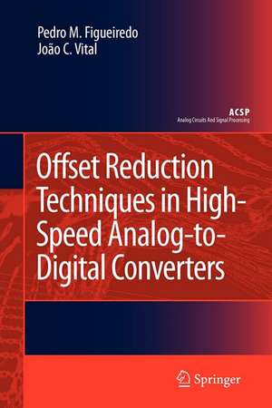
Offset Reduction Techniques in High-Speed Analog-to-Digital Converters analyzes, describes the design, and presents test results of Analog-to-Digital Converters (ADCs) employing the three main high-speed architectures: flash, two-step flash and folding and interpolation. The advantages and limitations of each one are reviewed, and the techniques employed to improve their performance are discussed.
Since the offset voltages of the constituting sub-blocks of these converters (pre-amplifiers, folding circuits and latched comparators) present the definitive linearity limitation, the offset is the fundamental design parameter in high-speed CMOS ADCs. Consequently, offset reduction techniques must be employed, in order to achieve high frequency operation with low power and layout area. Averaging and offset sampling are the most widely used, both being thoroughly characterized:
Since the offset voltages of the constituting sub-blocks of these converters (pre-amplifiers, folding circuits and latched comparators) present the definitive linearity limitation, the offset is the fundamental design parameter in high-speed CMOS ADCs. Consequently, offset reduction techniques must be employed, in order to achieve high frequency operation with low power and layout area. Averaging and offset sampling are the most widely used, both being thoroughly characterized:
- the most exhaustive study ever performed about averaging in both pre-amplifier and folding stages is presented, covering the DC and transient responses, all mismatch sources, termination, and a fully automated design procedure;
- existing offset sampling methods are carefully reviewed, and two new techniques are disclosed that, combined, yield a (nearly) offset free comparator.
Caracteristici
All high-speed ADC architectures (flash, two-step, folding and interpolation) covered in detail The performance parameters and trade-offs encountered in each of the ADC’s sub-blocks are analysed Most exhaustive study ever performed about averaging is presented Offset sampling techniques that yield a nearly offset free, high-speed, comparator are described
