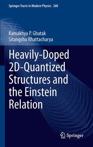
Heavily-Doped 2D-Quantized Structures and the Einstein Relation: Springer Tracts in Modern Physics, cartea 260
Autor Kamakhya P. Ghatak, Sitangshu Bhattacharyaen Limba Engleză Hardback – 11 aug 2014
| Toate formatele și edițiile | Preț | Express |
|---|---|---|
| Paperback (1) | 568.19 lei 38-44 zile | |
| Springer International Publishing – 23 aug 2016 | 568.19 lei 38-44 zile | |
| Hardback (1) | 579.15 lei 38-44 zile | |
| Springer International Publishing – 11 aug 2014 | 579.15 lei 38-44 zile |
Din seria Springer Tracts in Modern Physics
- 15%
 Preț: 648.42 lei
 - 18%
 Preț: 887.38 lei
 - 18%
 Preț: 1127.60 lei
 - 20%
 Preț: 814.68 lei
 - 20%
 Preț: 816.03 lei
 - 18%
 Preț: 1424.83 lei
 - 18%
 Preț: 785.55 lei
 -
 Preț: 409.63 lei
 -
 Preț: 428.30 lei
 -
 Preț: 426.34 lei
 -
 Preț: 387.38 lei
 -
 Preț: 387.20 lei
 -
 Preț: 381.21 lei
 -
 Preț: 378.71 lei
 -
 Preț: 382.95 lei
 -
 Preț: 384.48 lei
 -
 Preț: 382.36 lei
 -
 Preț: 387.38 lei
 -
 Preț: 391.40 lei
 -
 Preț: 380.63 lei
 -
 Preț: 386.00 lei
 - 18%
 Preț: 884.07 lei
 -
 Preț: 386.00 lei
 -
 Preț: 385.25 lei
 -
 Preț: 383.71 lei
 -
 Preț: 377.95 lei
 -
 Preț: 377.18 lei
 -
 Preț: 377.95 lei
 -
 Preț: 384.70 lei
 -
 Preț: 381.98 lei
 -
 Preț: 391.61 lei
 -
 Preț: 379.68 lei
 -
 Preț: 384.70 lei
 -
 Preț: 391.40 lei
 -
 Preț: 378.92 lei
 -
 Preț: 380.25 lei
 -
 Preț: 377.35 lei
 -
 Preț: 382.57 lei
 -
 Preț: 384.31 lei
 -
 Preț: 381.21 lei
 -
 Preț: 387.96 lei
 -
 Preț: 381.43 lei
 -
 Preț: 384.48 lei
 -
 Preț: 386.22 lei
 - 18%
 Preț: 1224.99 lei
Preț: 579.15 lei
Preț vechi: 723.93 lei
-20% Nou
Puncte Express: 869
Preț estimativ în valută:
110.82€ • 116.02$ • 91.70£
110.82€ • 116.02$ • 91.70£
Carte tipărită la comandă
Livrare economică 02-08 aprilie
Preluare comenzi: 021 569.72.76
Specificații
ISBN-13: 9783319083797
ISBN-10: 3319083791
Pagini: 387
Ilustrații: XL, 347 p. 58 illus.
Dimensiuni: 155 x 235 x 27 mm
Greutate: 0.72 kg
Ediția:2015
Editura: Springer International Publishing
Colecția Springer
Seria Springer Tracts in Modern Physics
Locul publicării:Cham, Switzerland
ISBN-10: 3319083791
Pagini: 387
Ilustrații: XL, 347 p. 58 illus.
Dimensiuni: 155 x 235 x 27 mm
Greutate: 0.72 kg
Ediția:2015
Editura: Springer International Publishing
Colecția Springer
Seria Springer Tracts in Modern Physics
Locul publicării:Cham, Switzerland
Public țintă
ResearchCuprins
From the Contents: The ER in Quantum Wells (QWs) of Heavily Doped(HD) Non-Parabolic Semiconductors.- The ER in NIPI Structures of HD Non-Parabolic Semiconductors.- The ER in Accumulation Layers of HD Non-Parabolic Semiconductors.- Suggestion for Experimental Determinations of 2D and 3D ERs and few Related Applications.- Conclusion and Scope for Future.
Notă biografică
Born in India in 1953, Professor K. P. Ghatak obtained his B.E degree in Electronics and Telecommunication Branch from the then Bengal Engineering College Shibpur (Presently Bengal Engineering and Science University) of the University of Calcutta in 1974, M.Tech degree from the Institute of Radio Physics and Electronics of the University of Calcutta in 1976. He obtained his PhD (Tech) degree from the University of Calcutta in 1988 on the basis of 27 published research papers in International peer-reviewed Scientific Journals which is still a record in the said Institute. He joined as Lecturer in the Institute of Radio Physics and Electronics of the University of Calcutta in 1983, Reader in the Department of Electronics and Telecommunication Engineering of Jadavpur University in 1987 and Professor in the Department of Electronic Science of the University of Calcutta in 1994 and was at the top of the merit list in all the cases respectively. From March 2012, he has joined in the Department of Electronics and Communication Engineering of National Institute of Technology, Agartala, Tripura and presently acting as the Professor and Head of the said Department. Professor K. P. Ghatak is the First Recipient of the Degree of Doctor of Engineering of Jadavpur University in 1991 since the University inception in 1955 and in the same year he received the Indian National Science Academy visiting fellowship to IIT-Kharagpur. He is the principal co-author of more than 300 research papers on Semiconductor Nano-science in eminent peer-reviewed International Journals and more than 50 research papers in the Proceedings of SPIE and MRS and many of his papers are being cited many times. Professor Ghatak is the invited Speaker of SPIE, MRS, etc., the referee and Associate Editor of different eminent Journals. He has produced more than two dozens of PhD candidates in various aspects of materials and nano-sciences and many of them are working as Dean, Professor, Associate Professor and Assistant Professor in different Universities and reputed Academic Institutions. He is the principal co-author of the SIX research monographs entitled "Einstein Relation in Compound Semiconductors and Their Nanostructures" Springer Series in Materials Science, Vol. 116, 2009, which is the first monograph on Einstein relation containing more than 100 open research problems, "Photoemission from Optoelectronic materials and their nanostructures", Springer Series in Nano structure Science and Technology, USA in 2009 as the first monograph solely devoted to Photoemission from nano-structured compounds containing more than 100 open research problems, "Thermo electric power in nano structured materials: Strong magnetic fields" Springer Series in Materials Science Vol. 137, 2010 which is the first monograph on this topic containing 150 open research problems, "Fowler-Nordheim Field Emission : Effects in Semiconductor Nanostructures "Springer Series in Solid State Sciences, Vol. 170, 2012 which is the first monograph on this topic containing 200 open research problems, "Effective electron mass in low dimensional semiconductors" Springer Series in Materials Science Vol. 167, 2013 which is the first monograph on this pin pointed topic containing 250 open research problems and "Debye Screening Length: "Effects of nano-structured materials" which is the first book solely devoted to Debye Screening Length: Effects of Nano-structured Materials containing more than 100 open research problems which will published in Springer Tracts in Modern Physics in late 2013 respectively. He is the Principal Editor of the two edited monographs entitled "Bismuth:: Characteristics, Production and Applications: Series in Materials Science and Technologies" and "Quantum Dots and Quantum Cellular Automata: Recent Trends and Applications : Series in Nanotechnology Science" of NOVA , USA respectively. The All Indian Council for Technical Education has selected the first Research and Developmentproject in his life for the best project award in Electronics and second best research project award considering all the branches of Engineering for the year 2006. In 2011, the University Grant Commission recommended a research project to him and placed him at the top in the list of awardees. His teaching interests are Non-Linear Network Analysis and Synthesis, Non-Linear Devices, Non-Linear Mechanics, Non- Linear Integral and Differential equations and present research interests are semiconductor nano science and number theory respectively. His brief CV has been enlisted in many biographical references of USA and UK.
Dr. Sitangshu Bhattacharya obtained his MSc and PhD degrees in 2003 and 2009 from the University of Calcutta and Jadavpur University respectively. He is the co-author of more than 50 scientific research paper in electro-thermal transport phenomena in semiconductor nanostructures in international peer reviewed journals and the said 6 research monographs. His present interest is electro thermal management in quantum effect devices and interconnects. He is presently working as an Assistant Professor in the Department of Electrical Engineering in Shiv Nadar University, India.
Dr. Sitangshu Bhattacharya obtained his MSc and PhD degrees in 2003 and 2009 from the University of Calcutta and Jadavpur University respectively. He is the co-author of more than 50 scientific research paper in electro-thermal transport phenomena in semiconductor nanostructures in international peer reviewed journals and the said 6 research monographs. His present interest is electro thermal management in quantum effect devices and interconnects. He is presently working as an Assistant Professor in the Department of Electrical Engineering in Shiv Nadar University, India.
Textul de pe ultima copertă
This book presents the Einstein Relation(ER) in two-dimensional (2-D) Heavily Doped(HD) Quantized Structures. The materials considered are quantized structures of HD non-linear optical, III-V, II-VI, Ge, Te, Platinum Antimonide, stressed materials, GaP, Gallium Antimonide, II-V, Bismuth Telluride together with various types of HD superlattices and their Quantized counterparts respectively. The ER in HD opto-electronic materials and their nanostructures is studied in the presence of strong light waves and intense electric fields on the basis of newly formulated electron dispersion laws that control the studies of such quantum effect devices. The suggestion for the experimental determination of HD 2D and 3D ERs and the importance of measurement of band gap in HD optoelectronic materials under intense built-in electric field in nanodevices and strong external photo excitation (for measuring photon induced physical properties) are also discussed in this context. The influence of crossed electric and quantizing magnetic fields on the ER of the different 2D HD quantized structures (quantum wells, inversion and accumulation layers, quantum well HD superlattices and nipi structures) under different physical conditions is discussed in detail. This monograph contains 100 open research problems which form the integral part of the text and are useful for both Ph.D aspirants and researchers in the fields of condensed matter physics, solid-state sciences, materials science, nano-science and technology and allied fields.
Caracteristici
Describes measurements of band gap in optoelectronic nanodevices under intense electric field and strong external photo excitation Presents 100 open research problems Covers a wide range of different technologically important electronic compounds in detail Includes supplementary material: sn.pub/extras
