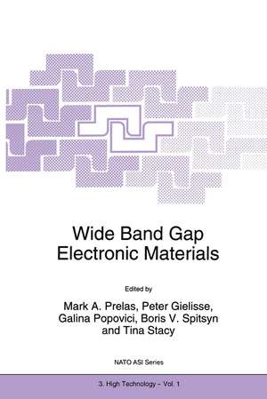
Wide Band Gap Electronic Materials: NATO Science Partnership Subseries: 3, cartea 1
Editat de Mark A. Prelas, Peter Gielisse, Galina Popovici, Boris V. Spitsyn, Tina Stacyen Limba Engleză Paperback – 13 oct 2012
| Toate formatele și edițiile | Preț | Express |
|---|---|---|
| Paperback (1) | 2099.91 lei 6-8 săpt. | |
| SPRINGER NETHERLANDS – 13 oct 2012 | 2099.91 lei 6-8 săpt. | |
| Hardback (1) | 2106.37 lei 6-8 săpt. | |
| SPRINGER NETHERLANDS – 31 mai 1995 | 2106.37 lei 6-8 săpt. |
Din seria NATO Science Partnership Subseries: 3
- 24%
 Preț: 1567.19 lei
 - 18%
 Preț: 2106.37 lei
 -
 Preț: 393.13 lei
 -
 Preț: 390.63 lei
 - 18%
 Preț: 1849.41 lei
 -
 Preț: 407.19 lei
 - 18%
 Preț: 1228.96 lei
 - 18%
 Preț: 1843.73 lei
 - 15%
 Preț: 642.51 lei
 -
 Preț: 402.76 lei
 - 18%
 Preț: 1829.86 lei
 -
 Preț: 379.48 lei
 - 18%
 Preț: 1224.54 lei
 -
 Preț: 401.42 lei
 - 18%
 Preț: 1841.68 lei
 -
 Preț: 391.99 lei
 - 18%
 Preț: 1234.46 lei
 -
 Preț: 405.28 lei
 -
 Preț: 396.62 lei
 - 18%
 Preț: 1226.73 lei
 - 18%
 Preț: 1233.52 lei
 - 18%
 Preț: 1228.62 lei
 - 5%
 Preț: 377.52 lei
 - 18%
 Preț: 1830.49 lei
 - 20%
 Preț: 336.21 lei
 - 18%
 Preț: 1225.48 lei
 -
 Preț: 397.38 lei
 - 18%
 Preț: 1830.65 lei
 - 15%
 Preț: 650.55 lei
 - 5%
 Preț: 1416.66 lei
Preț: 2099.91 lei
Preț vechi: 2560.86 lei
-18% Nou
Puncte Express: 3150
Preț estimativ în valută:
401.87€ • 414.59$ • 340.12£
401.87€ • 414.59$ • 340.12£
Carte tipărită la comandă
Livrare economică 05-19 martie
Preluare comenzi: 021 569.72.76
Specificații
ISBN-13: 9789401040785
ISBN-10: 9401040788
Pagini: 548
Ilustrații: XV, 531 p.
Dimensiuni: 160 x 240 x 29 mm
Greutate: 0.76 kg
Ediția:Softcover reprint of the original 1st ed. 1995
Editura: SPRINGER NETHERLANDS
Colecția Springer
Seria NATO Science Partnership Subseries: 3
Locul publicării:Dordrecht, Netherlands
ISBN-10: 9401040788
Pagini: 548
Ilustrații: XV, 531 p.
Dimensiuni: 160 x 240 x 29 mm
Greutate: 0.76 kg
Ediția:Softcover reprint of the original 1st ed. 1995
Editura: SPRINGER NETHERLANDS
Colecția Springer
Seria NATO Science Partnership Subseries: 3
Locul publicării:Dordrecht, Netherlands
Public țintă
ResearchCuprins
Diamond.- Problems of n-type Diamond Doping. Forced Methods of Doping.- Diffusion of Boron, Hydrogen, Oxygen and Lithium in Single Crystalline and Polycrystalline Diamond. A Novel Method for the Determination of the State of an Impurity: Forced Diffusion of Boron in IA Type Natural Diamond.- Chemical Aspects of Diamond Doping.- Diamond Growth by Hot Carbon Filament Chemical Vapor Deposition.- Diamond Particles on Silicon Tips: Preparation, Structure, and Field-Emission Properties.- To the Question of the Diamond Nuclei’s Formation from the Gas Phase.- Electrically and Optically Active Impurities and Defects in Diamond.- Prediction of Diamond Film Thermal Conductivity.- Spectral Hole-Burning Study of the Defects Created by Neutron Irradiation in a Natural Diamond.- Calculations of Phosphorous Electronic Levels in Diamond.- Hydrogen Chemistry on Diamond Surface.- Surface and Bulk Conductivity of Hydrogen Treated Polycrystalline Diamond.- Positron Annihilation in Diamond Films.- ESR Study of Paramagnetic Defects in Free Standing Diamond Films.- Efficient Reduction of Nitride and Nitrate to Ammonia Using B-doped Diamond Electrodes.- Electronic and Sensing Properties of Diamond.- Diamond MIS Capacitors With Silicon Dioxide Dielectric.- Diamond Photovoltaics: Characterization of CVD Diamond Film-Based Heterostructure for Light to Electricity Conversion.- Laser Modes in Diamond.- Advanced Applications of Diamond Electronics.- Laser-assisted Chemical Etching of Diamond Films in Oxygen.- Ion Milling of Polycrystalline Diamond Films.- Amorphous and Diamond-Kike Carbon Films.- Doping of Diamond-Like Carbon Films.- Unhydrogenated DLC Films Obtained by Magnetron Sputtering.- Simulation of Diffusion in an Amorphous Structure.- Optical and Electrical Properities ofQuantum-dimentional Multilayer Structures Based on Carbon Films.- Thermal Stability and Structural Reactions at the Tantalum/a-C Interface Under Vacuum Annealing Conditions.- Extended and Localized Electronic States in Tetrahedral Carbon Films.- Optical Properties of Sputtering and Glow Discharge a-C:H Films.- Application of Amorphous Hydrogenated Carbon Coating to Semiconductor Radiation Detectors.- Other Wide Bandgap Semiconductors.- Device for Growing and Doping in the Growth Process of Thin AlN Films.- Peculiarities of Chemical Vapor Heteroepitaxy of Wide Band Gap III-V Nitrides.- The Peculiarities of Cubic Boron Nitride Formation Mechanism Using Hexa-Ammonicate Boron Hydride of Magnesium.- Investigation of Cubic Boron Nitride Crystallization Processes in the BN-Li3N-(H, N) System.- Epitaxial Growth of AlN by Plasma Source Molecular Beam Epitaxy.- Electronic Structure and Related Properties of Tetrahedrally Bonded Wide-Band-Gap Materials Containing Early Elements of the Periodic Table.- Ion Implantation into Wide Bandgap Semiconductors.- Thermodynamic Properties of Boron Nitride.- Electrical Conductivity of Ceramic Based on Different Boron Nitride Modifications.- Cathodoluminescent Investigation of External Factors Influence on Defective Cubic Boron Nitride Structure.- Macro and Micro Structural Factors in Thin Film Growth of III-V Compounds.- The Features of the Sintering Process Under High Pressure of Aluminum Nitride Ceramic with High Thermal Conductivity.- Reactive Ion Etching of Silicon Carbide with Fluorine Containing Plasmas.- 1.54-µm Photoluminescence from Er-Implanted AlN & GaN.- AES-SIMS Analitical System for Compositional Measurements of Wide Band Gap Semiconductors.- Positron Annihilation in Sintered Boron Nitride.- Wide Band Gap Electronic Devices.-Wide Band-gap Photovoltaics.- Considerations in Further Development of Aluminum Nitrides as a Material for Device Applications.- Theoretical Aspects of Aluminum Nitride and Diamond in View of Laser and Photovoltaic Action.- Oral Presentations.- Poster Presentations.- List of Participants.- Affiliations Key.- Author Index.- Key Word Index.
