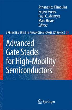
Advanced Gate Stacks for High-Mobility Semiconductors: Springer Series in Advanced Microelectronics, cartea 27
Editat de Athanasios Dimoulas, Evgeni Gusev, Paul C. McIntyre, Marc Heynsen Limba Engleză Hardback – 21 noi 2007
| Toate formatele și edițiile | Preț | Express |
|---|---|---|
| Paperback (1) | 949.73 lei 6-8 săpt. | |
| Springer Berlin, Heidelberg – 30 noi 2010 | 949.73 lei 6-8 săpt. | |
| Hardback (1) | 955.88 lei 6-8 săpt. | |
| Springer Berlin, Heidelberg – 21 noi 2007 | 955.88 lei 6-8 săpt. |
Din seria Springer Series in Advanced Microelectronics
- 15%
 Preț: 645.79 lei
 - 18%
 Preț: 951.59 lei
 - 20%
 Preț: 645.31 lei
 - 15%
 Preț: 643.34 lei
 - 18%
 Preț: 1007.35 lei
 - 18%
 Preț: 1234.77 lei
 - 15%
 Preț: 641.03 lei
 - 18%
 Preț: 954.45 lei
 - 15%
 Preț: 641.20 lei
 - 18%
 Preț: 1842.94 lei
 - 15%
 Preț: 639.84 lei
 - 18%
 Preț: 1051.98 lei
 - 18%
 Preț: 955.70 lei
 - 18%
 Preț: 953.82 lei
 - 15%
 Preț: 638.24 lei
 - 18%
 Preț: 1110.55 lei
 -
 Preț: 387.20 lei
 - 15%
 Preț: 642.68 lei
 - 18%
 Preț: 956.81 lei
 - 15%
 Preț: 642.03 lei
 - 18%
 Preț: 947.35 lei
 - 15%
 Preț: 632.70 lei
 - 18%
 Preț: 936.95 lei
 - 18%
 Preț: 946.87 lei
 - 18%
 Preț: 1559.80 lei
 - 15%
 Preț: 633.53 lei
Preț: 955.88 lei
Preț vechi: 1165.70 lei
-18% Nou
Puncte Express: 1434
Preț estimativ în valută:
182.95€ • 190.28$ • 153.32£
182.95€ • 190.28$ • 153.32£
Carte tipărită la comandă
Livrare economică 13-27 martie
Preluare comenzi: 021 569.72.76
Specificații
ISBN-13: 9783540714903
ISBN-10: 3540714901
Pagini: 408
Ilustrații: XXII, 384 p.
Dimensiuni: 155 x 235 x 26 mm
Greutate: 0.74 kg
Ediția:2007
Editura: Springer Berlin, Heidelberg
Colecția Springer
Seria Springer Series in Advanced Microelectronics
Locul publicării:Berlin, Heidelberg, Germany
ISBN-10: 3540714901
Pagini: 408
Ilustrații: XXII, 384 p.
Dimensiuni: 155 x 235 x 26 mm
Greutate: 0.74 kg
Ediția:2007
Editura: Springer Berlin, Heidelberg
Colecția Springer
Seria Springer Series in Advanced Microelectronics
Locul publicării:Berlin, Heidelberg, Germany
Public țintă
ResearchCuprins
Strained-Si CMOS Technology.- High Current Drivability MOSFET Fabricated on Si(110) Surface.- Advanced High-Mobility Semiconductor-on-Insulator Materials.- Passivation and Characterization of Germanium Surfaces.- Interface Engineering for High-? Ge MOSFETs.- Effect of Surface Nitridation on the Electrical Characteristics of Germanium High-?/Metal Gate Metal-Oxide-Semiconductor Devices.- Modeling of Growth of High-? Oxides on Semiconductors.- Physical, Chemical, and Electrical Characterization of High-? Dielectrics on Ge and GaAs.- Point Defects in Stacks of High-? Metal Oxides on Ge: Contrast with the Si Case.- High ? Gate Dielectrics for Compound Semiconductors.- Interface Properties of High-? Dielectrics on Germanium.- A Theoretical View on the Dielectric Properties of Crystalline and Amorphous High-? Materials and Films.- Germanium Nanodevices and Technology.- Opportunities and Challenges of Germanium Channel MOSFETs.- Germanium Deep-Submicron p-FET and n-FET Devices, Fabricated on Germanium-On-Insulator Substrates.- Processing and Characterization of III–V Compound Semiconductor MOSFETs Using Atomic Layer Deposited Gate Dielectrics.- Fabrication of MBE High-? MOSFETs in a Standard CMOS Flow.
Notă biografică
Dr. Dimoulas obtained his Ph.D in Applied Physics from the University of Crete and the Foundation for Research &Technology-Hellas (FORTH), Greece in 1991 for his research on heteroepitaxial strain of III-V semiconductors grown on Si by MBE. He worked in the Microelectronics Research Group of FORTH until 1992. He was Human Capital & Mobility Fellow of the EU at the University of Groningen, Holland until 1994, a Research Fellow at the California Institute of Technology (CALTECH), Chemical Engineering, Pasadena USA until1996 and member of the Faculty at the University of Maryland at College Park (UMCP) USA, until February 1999. In addition, he has been visiting research scientist at NRL, Washington DC in 1992 and at IBM Zurich Research Laboratory, Switzerland in 2006. Since 1999, he is research director and head of the MBE laboratory at the Institute of Materials Science of the National Center for Scientific Research DEMOKRITOS, Athens, Greece. He is leading several European-funded projects in the areas of advanced microelectronic materials and devices. He has co-author more than 80 publications in international journals, archives and proceedings, and has also written book chapters. He has given 15 invited presentations during the last five years. He has been involved in the organization of several conferences and workshops either as the main organizer or as a member of advisory and program committees. Finally, he is reviewer in recognized International Journals and evaluator of research and development projects. His expertise includes MBE growth of Semiconductor and dielectric materials (high-k oxides), nanodevice processing by e-beam lithography and materials characterization and device electrical testing. His current interests focus on advanced high-k gate stacks for Ge and III-V MOS technology
Dr. Evgeni Gusev received his MS (Applied Physics/Molecular Physics) and PhD (Solid State Physics) from Moscow Engineering Physics Institute – TechnicalUniversity in 1988 and 1991. In 1993, he joined Laboratory for Surface Modifications at Rutgers University, first as a PostDoctoral Fellow and then as a Research Assistant Professor, where he established a program on fundamental aspects of gate dielectrics. In 1997, following the invitation by Prof. Masataka Hirose, he held an appointment of Visiting Professor in the Center for Nanodevices and Systems in Hiroshima University, Japan. Shortly after that he moved to IBM, where he was responsible for several projects on gate stack processing, characterization, and FEOL device integration (starting from 0.25um CMOS to 32 nm devices more recently) in both IBM Semiconductor Research and Development Center (SRDC) in East Fishkill (NY) and IBM T.J. Watson Research Center in Yorktown Heights (NY). In July 2005, he joined QUALCOMM MEMS Technology Development Center in San Jose as the Director of Research and Development. Since 2004, he is also a Distinguished Visiting Professor at Rutgers University. Dr. Gusev has contributed to the technical R&D community with 10 edited books, more than 150 publications and 20 issued and filed patents on various aspects of semiconductor devices and technology. He is a member of several international professional committees, panels and societies.
Professor Paul McIntyre is Associate Professor of Materials Science and Engineering and Deputy Director of the Geballe Laboratory for Advanced Materials at Stanford University. McIntyre leads a research team of fourteen graduate students, three visiting scientists, and two consulting professors who perform basic research on nanostructured inorganic materials for applications in electronics, energy technologies and sensors. He is best known for his work on metal oxide/semiconductor interfaces, ultrathin high-k dielectrics, defects in complex metal oxide thin films, and nanostructured Si-Ge single crystals. His research team synthesizes materials, characterizestheir structures and compositions with a variety of advanced microscopies and spectroscopies, studies the passivation of their interfaces, and measures functional properties of devices. Their research is supported by several U.S. government agencies and major semiconductor manufacturers world-wide. McIntyre is an author of approximately 100 archival journal papers and inventor of 5 US patents, and has given over 60 invited presentations, plenary talks and tutorial lectures. He has received an IBM Faculty Award and Charles Lee Powell Foundation Faculty Scholarship in recognition of his group’s research. Prior to joining Stanford, McIntyre was a member of the technical staff in the Central Research Laboratories at Texas Instruments and he also served as Lab Director’s Fund Postdoctoral Fellow in the Materials Division at Los Alamos National Laboratory. He earned the Sc.D. from the Materials Science and Engineering department at MIT and the B.A.Sc. from the Materials Engineering department at the University of British Columbia (Canada). McIntyre is a technical advisor to Unity Semiconductor Corporation, and has been an invited member of government and industry panels studying future research needs in ceramic materials, metal oxide/semiconductor structures, nano-scale ferroelectrics and nano-electronics.
Professor Dr. Marc Heyns was born in Turnhout, Belgium, on November 16, 1956. He received the M.S. degree in Applied Sciences (Electronics) in 1979 from the Katholieke Universiteit Leuven, Belgium. In 1986 he received the Ph.D. degree, also from the Katholieke Universiteit Leuven, Belgium, with a thesis entitled: "Study of the charge trapping and degradation of thermally grown SiO2 layers". From 1979 to 1985 he held a fellowship from the National Fund for Scientific Research (NFWO) in the Laboratory for Physics and Electronics of Semiconductors of the K.U. Leuven. In January 1986 he joined IMEC where he became Department Director and ProgramDirector responsible for a research group working on ultra-clean processing technology, advanced high-k gate stacks, metal gates, epitaxial deposition of materials, environmentally benign processing and novel high-mobility substrate materials. He became an IMEC-Fellow in 2001 and a Professor at the Katholieke Universiteit Leuven in 2005. He has authored or co-authored more than 150 contributions in scientific journals and more than 500 papers at international conferences. His current research topics include novel high-k dielectric materials, advanced cleaning and surface preparation technology, epitaxy, novel devices made on high-mobility substrates such Ge and III/V compounds, nanowires and carbon nanotubes.
Textul de pe ultima copertă
Will nanoelectronic devices continue to scale according to Moore’s law? At this moment, there is no easy answer since gate scaling is rapidly emerging as a serious roadblock for the evolution of CMOS technology. Channel engineering based on high-mobility semiconductor materials (e.g. strained Si, alternative orientation substrates, Ge or III-V compounds) could help overcome the obstacles since they offer performance enhancement. There are several concerns though. Do we know how to make complex engineered substrates (e.g. Germanium-on-Insulator)? Which are the best interface passivation methodologies and (high-k) gate dielectrics on Ge and III-V compounds? Can we process these materials in short channel transistors using flows, toolsets and know how similar to that in Si technology? How do these materials and devices behave at the nanoscale? The reader will get a clear view of what has been done so far, what is the state-of-the-art and which are the main challenges ahead before we come any close to a viable Ge and III-V MOS technology.
Caracteristici
Comprehensive monograph on gate stacks in semiconductor technology Covers the major latest developments and basics A reference work for researchers, engineers and graduate students alike Includes supplementary material: sn.pub/extras


