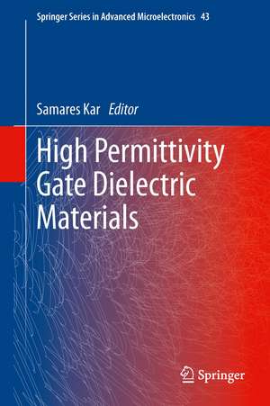
High Permittivity Gate Dielectric Materials: Springer Series in Advanced Microelectronics, cartea 43
Editat de Samares Karen Limba Engleză Hardback – 8 iul 2013
.
| Toate formatele și edițiile | Preț | Express |
|---|---|---|
| Paperback (1) | 955.25 lei 6-8 săpt. | |
| Springer Berlin, Heidelberg – 23 aug 2016 | 955.25 lei 6-8 săpt. | |
| Hardback (1) | 810.76 lei 38-44 zile | |
| Springer Berlin, Heidelberg – 8 iul 2013 | 810.76 lei 38-44 zile |
Din seria Springer Series in Advanced Microelectronics
- 15%
 Preț: 645.79 lei
 - 24%
 Preț: 1571.35 lei
 - 18%
 Preț: 951.59 lei
 - 20%
 Preț: 645.31 lei
 - 15%
 Preț: 643.34 lei
 - 18%
 Preț: 1007.35 lei
 - 18%
 Preț: 1229.38 lei
 - 15%
 Preț: 641.03 lei
 - 18%
 Preț: 954.45 lei
 - 15%
 Preț: 641.20 lei
 - 18%
 Preț: 1842.94 lei
 - 15%
 Preț: 639.84 lei
 - 18%
 Preț: 1051.98 lei
 - 18%
 Preț: 955.70 lei
 - 18%
 Preț: 953.82 lei
 - 15%
 Preț: 638.24 lei
 - 18%
 Preț: 1110.55 lei
 -
 Preț: 387.20 lei
 - 15%
 Preț: 642.68 lei
 - 18%
 Preț: 956.81 lei
 - 15%
 Preț: 642.03 lei
 - 18%
 Preț: 947.35 lei
 - 18%
 Preț: 955.88 lei
 - 15%
 Preț: 632.70 lei
 - 18%
 Preț: 936.95 lei
 - 18%
 Preț: 946.87 lei
 - 18%
 Preț: 1559.80 lei
 - 15%
 Preț: 638.43 lei
Preț: 810.76 lei
Preț vechi: 1066.79 lei
-24% Nou
Puncte Express: 1216
Preț estimativ în valută:
155.19€ • 168.63$ • 130.44£
155.19€ • 168.63$ • 130.44£
Carte tipărită la comandă
Livrare economică 17-23 aprilie
Preluare comenzi: 021 569.72.76
Specificații
ISBN-13: 9783642365348
ISBN-10: 3642365345
Pagini: 524
Ilustrații: XXXII, 489 p. 325 illus., 168 illus. in color.
Dimensiuni: 155 x 235 x 38 mm
Greutate: 0.86 kg
Ediția:2013
Editura: Springer Berlin, Heidelberg
Colecția Springer
Seria Springer Series in Advanced Microelectronics
Locul publicării:Berlin, Heidelberg, Germany
Public țintă
Professional/practitionerCuprins
Historical Perspectives.- High Mobility Channels.- Non-Volatile Memory.- Hafnium-Based Gate Dielectric Materials.- Lanthanum-Based High-K Gate Dielectric Materials.- Crystalline High-K Gate Dielectric Materials.- High-K Gate Dielectric Processing.- Metal Gate Electrodes.- Flat-Band/Threshold Voltage Control.- Interfaces and Defects.- Electrical Characterization and Parameter Extraction.- Non-Contact Metrology of High-K Gate Dielectrics.- Channel Mobility.- High-K Gate Dielectric Reliability Issues.- Bias Temperature Instability.- Integration Issues.
Notă biografică
Samares Kar was born in Kolkata, India in 1942. He received the B.Tech. degree in electrical engineering in 1962 from the Indian Institute of Technology in Kharagpur, India, and the M.S. and Ph.D. degrees in electrical engineering from Lehigh University in Bethlehem, Pennsylvania, USA in 1968 and 1970, respectively.
During the period 1963-1965, he worked in West Germany, first as a design engineer with the Hamburger Transformatorenbau in Hamburg, and then as a project engineer with the Continental Elektroindustrie in Rheydt. During the period 1971-1974, he was a member of the scientific staff at the Fraunhofer Institute of Applied Solid State Physics in Freiburg, West Germany. In 1975, he joined the Indian Institute of Technology in Kanpur, where he was a professor of electrical engineering and materials science from 1980 till 2004, an emeritus fellow between 2004 and 2006, and currently is an R & D consultant. In 1979, he was at The Pennsylvania State University, University Park, Pennsylvania as a visiting associate professor of engineering science, and in 1981, he was at Lehigh University, Bethlehem as a visiting professor of electrical engineering. His research interests have included MOS tunnel devices, Si-SiO2 interface states, solar cells, ion-beam induced defects, organic monolayers, high-K gate dielectrics, and MOS/MIS parameter extraction. His seminal work on ultrathin (2-4 nm) SiO2 gate dielectrics, carried out more than three decades ago, provides some basic theory and tools for the current and future generation MOS nano-transistors, in particular, on issues related to the ultimate gate dielectric thinness, electrical characterization, and metal-related interface states.
Dr. Kar was/is the lead organizer of The First, Second, Third, Fourth, and Fifth International Symposium on High Dielectric Constant Materials held respectively in October 2002 in Salt Lake City, UT, in October 2003 in Orlando, FL, in October 2005 in Los Angeles, CA., in October 2006 in Cancun, Mexico, and in October 2007 in Washington, DC. He is the lead editor of the four volumes of the book entitled "Physics and Technology of High-K Gate Dielectrics".
Textul de pe ultima copertă
"The book comprehensively covers all the current and the emerging areas of the physics and the technology of high permittivity gate dielectric materials, including, topics such as MOSFET basics and characteristics, hafnium-based gate dielectric materials, Hf-based gate dielectric processing, metal gate electrodes, flat-band and threshold voltage tuning, channel mobility, high-k gate stack degradation and reliability, lanthanide-based high-k gate stack materials, ternary hafnia and lanthania based high-k gate stack films, crystalline high-k oxides, high mobility substrates, and parameter extraction. Each chapter begins with the basics necessary for understanding the topic, followed by a comprehensive review of the literature, and ultimately graduating to the current status of the technology and our scientific understanding and the future prospects."
Caracteristici
Most advanced and comprehensive book on high permittivity gate dielectrics Covers the basics, latest developments, and applications A reference work for researchers, electrical engineers and materials scientists as well as a study text for master and doctor course students Includes supplementary material: sn.pub/extras
