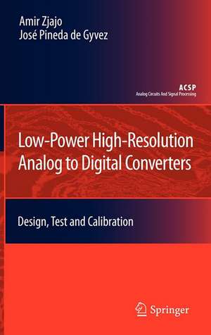
Low-Power High-Resolution Analog to Digital Converters: Design, Test and Calibration: Analog Circuits and Signal Processing
Autor Amir Zjajo, José Pineda de Gyvezen Limba Engleză Hardback – 5 noi 2010
In an attempt to address these issues, Low-Power High-Resolution Analog-to-Digital Converters specifically focus on: i) improving the power efficiency for the high-speed, and low spurious spectral A/D conversion performance by exploring the potential of low-voltage analog design and calibration techniques, respectively, and ii) development of circuit techniques and algorithms to enhance testing and debugging potential to detect errors dynamically, to isolate and confine faults, and to recover errors continuously. The feasibility of the described methods has been verified by measurementsfrom the silicon prototypes fabricated in standard 180nm, 90nm and 65nm CMOS technology.
| Toate formatele și edițiile | Preț | Express |
|---|---|---|
| Paperback (1) | 389.31 lei 6-8 săpt. | |
| SPRINGER NETHERLANDS – 23 aug 2016 | 389.31 lei 6-8 săpt. | |
| Hardback (1) | 396.62 lei 6-8 săpt. | |
| SPRINGER NETHERLANDS – 5 noi 2010 | 396.62 lei 6-8 săpt. |
Din seria Analog Circuits and Signal Processing
- 5%
 Preț: 902.97 lei
 - 9%
 Preț: 628.98 lei
 -
 Preț: 388.34 lei
 - 15%
 Preț: 636.30 lei
 - 15%
 Preț: 636.80 lei
 - 18%
 Preț: 941.82 lei
 - 15%
 Preț: 639.08 lei
 - 18%
 Preț: 918.48 lei
 - 15%
 Preț: 631.21 lei
 - 15%
 Preț: 642.03 lei
 - 15%
 Preț: 641.85 lei
 - 18%
 Preț: 887.05 lei
 - 18%
 Preț: 944.51 lei
 - 15%
 Preț: 632.55 lei
 - 15%
 Preț: 641.03 lei
 - 18%
 Preț: 836.39 lei
 - 15%
 Preț: 642.18 lei
 - 15%
 Preț: 639.90 lei
 - 18%
 Preț: 947.85 lei
 - 15%
 Preț: 642.51 lei
 - 15%
 Preț: 631.86 lei
 - 15%
 Preț: 634.49 lei
 - 15%
 Preț: 635.47 lei
 - 15%
 Preț: 640.06 lei
 - 15%
 Preț: 631.53 lei
 - 15%
 Preț: 635.65 lei
 - 18%
 Preț: 941.50 lei
 - 18%
 Preț: 1112.92 lei
 - 15%
 Preț: 636.30 lei
 - 15%
 Preț: 633.19 lei
 - 15%
 Preț: 635.80 lei
 - 18%
 Preț: 888.01 lei
 - 18%
 Preț: 942.76 lei
 - 18%
 Preț: 1387.10 lei
 - 18%
 Preț: 1115.28 lei
 - 15%
 Preț: 633.68 lei
 - 15%
 Preț: 641.03 lei
 - 15%
 Preț: 638.57 lei
 - 15%
 Preț: 642.51 lei
 - 18%
 Preț: 947.85 lei
 - 15%
 Preț: 640.71 lei
 - 15%
 Preț: 640.88 lei
 - 15%
 Preț: 631.40 lei
 - 18%
 Preț: 944.19 lei
 - 18%
 Preț: 944.67 lei
 - 18%
 Preț: 942.94 lei
 - 15%
 Preț: 641.20 lei
 - 20%
 Preț: 555.52 lei
 - 18%
 Preț: 1003.38 lei
Preț: 396.62 lei
Nou
Puncte Express: 595
Preț estimativ în valută:
75.90€ • 78.41$ • 63.17£
75.90€ • 78.41$ • 63.17£
Carte tipărită la comandă
Livrare economică 26 martie-09 aprilie
Preluare comenzi: 021 569.72.76
Specificații
ISBN-13: 9789048197248
ISBN-10: 9048197244
Pagini: 250
Ilustrații: XX, 293 p.
Dimensiuni: 155 x 235 x 28 mm
Greutate: 0.62 kg
Ediția:2011
Editura: SPRINGER NETHERLANDS
Colecția Springer
Seria Analog Circuits and Signal Processing
Locul publicării:Dordrecht, Netherlands
ISBN-10: 9048197244
Pagini: 250
Ilustrații: XX, 293 p.
Dimensiuni: 155 x 235 x 28 mm
Greutate: 0.62 kg
Ediția:2011
Editura: SPRINGER NETHERLANDS
Colecția Springer
Seria Analog Circuits and Signal Processing
Locul publicării:Dordrecht, Netherlands
Public țintă
ResearchCuprins
Foreword.- Abbrevations.- Symbols.- 1. Introduction.- 2. Analog to Digital Conversion.- 3. Design of Multi-Step A/D Converters.- 4. Multi-Step A/D Converter Testing.- 5. Multi-Step A/D Converter Debugging.- 6. Conclusions and Recommendations.- Appendix.- References.- Index.-
Notă biografică
Amir Zjajo received the M.Sc. and DIC degrees from the Imperial College London, London, U.K., in 2000 and PhD degree from Eindhoven University of Technology in 2010, all in the electrical engineering. In 2000, he joined Philips Research Laboratories, Eindhoven, The Netherlands, as a member of the research staff in the Mixed-Signal Circuits and Systems Group. From 2006 until 2009, he was with Corporate Research of NXP Semiconductors as a senior research scientist. In 2009, he joined Delft University of Technology as a Faculty member in the Circuit and Systems Group. Dr. Zjajo has published more then 20 papers in referenced journals and conference proceedings, and holds 2 patents with 7 more pending. He serves as a member of Technical Program Committee of IEEE Design, Automation and Test in Europe Conference, and IEEE International Mixed-Signal Circuits, Sensors and Systems Workshop. His research interests include mixed-signal circuit design, signal integrity and timing and yield optimization of VLSI.
José Pineda de Gyvez received the Ph.d. degree from the Eindhoven University of Technology, The Netherlands, in 1991. From 1991 until 1999 he was a Faculty member in the Department of Electrical Engineering at Texas A&M University, USA. He is currently a Senior Principal at NXP Semiconductors in The Netherlands. Since 2006 he also holds the professorship “Deep Submicron Integration” in the Department of Electrical Engineering at the Eindhoven University of Technology. Dr. Pineda de Gyvez has been Associate Editor in IEEE Transactions on Circuits and Systems Part I and Part II, and also Associate Editor for Technology in IEEE Transactions on Semiconductor Manufacturing. He is also a member of the editorial board of the Journal of Low Power Electronics. Dr. Pineda has more than 100 combined publications in the fields of testing, nonlinear circuits, and low power design. He is (co)-author of three books, and has a number of grantedpatents. His work has been acknowledged in academic environments as well as in patent portfolios of many companies. Pineda’s research has been funded by the Dutch Ministry of Science, US Office of Naval Research, US National Science Foundation, among others. Dr. Pineda is an IEEE Fellow.
José Pineda de Gyvez received the Ph.d. degree from the Eindhoven University of Technology, The Netherlands, in 1991. From 1991 until 1999 he was a Faculty member in the Department of Electrical Engineering at Texas A&M University, USA. He is currently a Senior Principal at NXP Semiconductors in The Netherlands. Since 2006 he also holds the professorship “Deep Submicron Integration” in the Department of Electrical Engineering at the Eindhoven University of Technology. Dr. Pineda de Gyvez has been Associate Editor in IEEE Transactions on Circuits and Systems Part I and Part II, and also Associate Editor for Technology in IEEE Transactions on Semiconductor Manufacturing. He is also a member of the editorial board of the Journal of Low Power Electronics. Dr. Pineda has more than 100 combined publications in the fields of testing, nonlinear circuits, and low power design. He is (co)-author of three books, and has a number of grantedpatents. His work has been acknowledged in academic environments as well as in patent portfolios of many companies. Pineda’s research has been funded by the Dutch Ministry of Science, US Office of Naval Research, US National Science Foundation, among others. Dr. Pineda is an IEEE Fellow.
Textul de pe ultima copertă
With the fast advancement of CMOS fabrication technology, more and more signal-processing functions are implemented in the digital domain for a lower cost, lower power consumption, higher yield, and higher re-configurability. This has recently generated a great demand for low-power, low-voltage A/D converters that can be realized in a mainstream deep-submicron CMOS technology. However, the discrepancies between lithography wavelengths and circuit feature sizes are increasing. Lower power supply voltages significantly reduce noise margins and increase variations in process, device and design parameters. Consequently, it is steadily more difficult to control the fabrication process precisely enough to maintain uniformity. The inherent randomness of materials used in fabrication at nanoscopic scales means that performance will be increasingly variable, not only from die-to-die but also within each individual die. Parametric variability will be compounded by degradation in nanoscale integrated circuits resulting in instability of parameters over time, eventually leading to the development of faults. Process variation cannot be solved by improving manufacturing tolerances; variability must be reduced by new device technology or managed by design in order for scaling to continue. Similarly, within-die performance variation also imposes new challenges for test methods.
In an attempt to address these issues, Low-Power High-Resolution Analog-to-Digital Converters specifically focus on: i) improving the power efficiency for the high-speed, and low spurious spectral A/D conversion performance by exploring the potential of low-voltage analog design and calibration techniques, respectively, and ii) development of circuit techniques and algorithms to enhance testing and debugging potential to detect errors dynamically, to isolate and confine faults, and to recover errors continuously. The feasibility of the described methods has been verified by measurementsfrom the silicon prototypes fabricated in standard 180nm, 90nm and 65nm CMOS technology.
In an attempt to address these issues, Low-Power High-Resolution Analog-to-Digital Converters specifically focus on: i) improving the power efficiency for the high-speed, and low spurious spectral A/D conversion performance by exploring the potential of low-voltage analog design and calibration techniques, respectively, and ii) development of circuit techniques and algorithms to enhance testing and debugging potential to detect errors dynamically, to isolate and confine faults, and to recover errors continuously. The feasibility of the described methods has been verified by measurementsfrom the silicon prototypes fabricated in standard 180nm, 90nm and 65nm CMOS technology.
Caracteristici
Unique combination of design, test, debugging and calibration of A/D converters (probably only on the market) Numerous examples and easy to follow procedure for design, test, debugging and calibration of A/D converters Both state-of-the art software and hardware implementations and their chip realizations are given Includes supplementary material: sn.pub/extras
