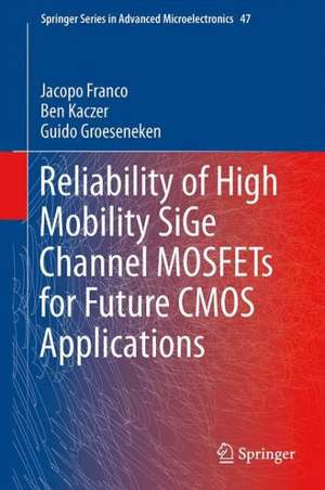
Reliability of High Mobility SiGe Channel MOSFETs for Future CMOS Applications: Springer Series in Advanced Microelectronics, cartea 47
Autor Jacopo Franco, Ben Kaczer, Guido Groesenekenen Limba Engleză Hardback – 29 oct 2013
This book focuses on the reliability of the novel (Si)Ge channel quantum well pMOSFET technology. This technology is being considered for possible implementation in next CMOS technology nodes, thanks to its benefit in terms of carrier mobility and device threshold voltage tuning. We observe that it also opens a degree of freedom for device reliability optimization. By properly tuning the device gate stack, sufficiently reliable ultra-thin EOT devices with a 10 years lifetime at operating conditions are demonstrated.
The extensive experimental datasets collected on a variety of processed 300mm wafers and presented here show the reliability improvement to be process - and architecture-independent and, as such, readily transferable to advanced device architectures as Tri-Gate (finFET) devices. We propose a physical model to understand the intrinsically superior reliability of the MOS system consisting of a Ge-based channel and a SiO2/HfO2 dielectric stack.
The improved reliability properties here discussed strongly support (Si)Ge technology as a clear frontrunner for future CMOS technology nodes.
| Toate formatele și edițiile | Preț | Express |
|---|---|---|
| Paperback (1) | 553.25 lei 38-44 zile | |
| SPRINGER NETHERLANDS – 23 aug 2016 | 553.25 lei 38-44 zile | |
| Hardback (1) | 642.18 lei 43-57 zile | |
| SPRINGER NETHERLANDS – 29 oct 2013 | 642.18 lei 43-57 zile |
Din seria Springer Series in Advanced Microelectronics
- 15%
 Preț: 645.79 lei
 - 18%
 Preț: 951.59 lei
 - 20%
 Preț: 645.31 lei
 - 15%
 Preț: 643.34 lei
 - 18%
 Preț: 1007.35 lei
 - 18%
 Preț: 1229.38 lei
 - 15%
 Preț: 641.03 lei
 - 18%
 Preț: 954.45 lei
 - 15%
 Preț: 641.20 lei
 - 18%
 Preț: 1842.94 lei
 - 15%
 Preț: 639.84 lei
 - 18%
 Preț: 1051.98 lei
 - 18%
 Preț: 955.70 lei
 - 18%
 Preț: 953.82 lei
 - 15%
 Preț: 638.24 lei
 - 18%
 Preț: 1110.55 lei
 -
 Preț: 387.20 lei
 - 15%
 Preț: 642.68 lei
 - 18%
 Preț: 956.81 lei
 - 15%
 Preț: 642.03 lei
 - 18%
 Preț: 947.35 lei
 - 18%
 Preț: 955.88 lei
 - 15%
 Preț: 632.70 lei
 - 18%
 Preț: 936.95 lei
 - 18%
 Preț: 946.87 lei
 - 18%
 Preț: 1559.80 lei
 - 15%
 Preț: 633.53 lei
Preț: 642.18 lei
Preț vechi: 755.51 lei
-15% Nou
Puncte Express: 963
Preț estimativ în valută:
122.88€ • 128.64$ • 101.68£
122.88€ • 128.64$ • 101.68£
Carte tipărită la comandă
Livrare economică 07-21 aprilie
Preluare comenzi: 021 569.72.76
Specificații
ISBN-13: 9789400776623
ISBN-10: 9400776624
Pagini: 208
Ilustrații: XIX, 187 p. 219 illus.
Dimensiuni: 155 x 235 x 17 mm
Greutate: 0.47 kg
Ediția:2014
Editura: SPRINGER NETHERLANDS
Colecția Springer
Seria Springer Series in Advanced Microelectronics
Locul publicării:Dordrecht, Netherlands
ISBN-10: 9400776624
Pagini: 208
Ilustrații: XIX, 187 p. 219 illus.
Dimensiuni: 155 x 235 x 17 mm
Greutate: 0.47 kg
Ediția:2014
Editura: SPRINGER NETHERLANDS
Colecția Springer
Seria Springer Series in Advanced Microelectronics
Locul publicării:Dordrecht, Netherlands
Public țintă
ResearchCuprins
1 Introduction.- 2 Degradation mechanisms.- 3 Techniques and devices.- 4 Negative Bias Temperature Instability in (Si)Ge pMOSFETs.- 5 Negative Bias Temperature Instability in nanoscale devices.- 6 Channel Hot Carriers and other reliability mechanisms.- 7 Conclusions and perspectives.
Notă biografică
Jacopo Franco received the M.Sc. in Electronic Engineering from Università della Calabria, Italy, in 2008 and the Ph.D. degree in Engineering from the KU Leuven, Belgium, in 2013. He is currently a Researcher in the reliability group of imec, Leuven, Belgium. His research interests focus on the reliability of high-mobility channel transistors for future CMOS nodes and on variability issues in nanoscale devices. He has co-authored more than 70 papers in international journal and conference proceedings and received the Best Student Paper Award at SISC (2009), the EDS Ph.D. Student Fellowship (2012), the EDS Paul Rappaport Award (2011), and the Best Paper Award at IRPS (2012).
Ben Kaczer is a Principal Scientist at imec, Belgium. He received the M.S. degree in Physical Electronics from Charles University, Prague, in 1992 and the M.S. and Ph.D. degrees in Physics from The Ohio State University, in 1996 and 1998, respectively. In 1998 he joined the reliability group of imec. He has co-authored more than 300 papers and received 5 Best or Outstanding IRPS and 1 IPFA Paper Awards. He is currently serving on the IEEE T. Electron Dev. Editorial Board.
Guido Groeseneken received the M.Sc. degree in 1980 and the Ph.D degree in applied sciences in 1986, both from the KU Leuven, Belgium. In 1987 he joined the R&D Laboratory of imec, Leuven, Belgium, where he is responsible for research in reliability physics for deep submicron CMOS technologies and in nanotechnology for post-CMOS applications. Since 2001 he is Professor at the KU Leuven, where he is Program Director of the Master in Nanoscience and Nanotechnology and coordinating a European Erasmus Mundus Master program in Nanoscience and nanotechnology. He became an IEEE Fellow in 2005 and an IMEC Fellow in 2007.
Textul de pe ultima copertă
Due to the ever increasing electric fields in scaled CMOS devices, reliability is becoming a showstopper for further scaled technology nodes. Although several groups have already demonstrated functional Si channel devices with aggressively scaled Equivalent Oxide Thickness (EOT) down to 5Å, a 10 year reliable device operation cannot be guaranteed anymore due to severe Negative Bias Temperature Instability.
This book focuses on the reliability of the novel (Si)Ge channel quantum well pMOSFET technology. This technology is being considered for possible implementation in next CMOS technology nodes, thanks to its benefit in terms of carrier mobility and device threshold voltage tuning. We observe that it also opens a degree of freedom for device reliability optimization. By properly tuning the device gate stack, sufficiently reliable ultra-thin EOT devices with a 10 years lifetime at operating conditions are demonstrated.
The extensive experimental datasets collected on a variety of processed 300mm wafers and presented here show the reliability improvement to be process- and architecture-independent and, as such, readily transferable to advanced device architectures as Tri-Gate (finFET) devices. We propose a physical model to understand the intrinsically superior reliability of the MOS system consisting of a Ge-based channel and a SiO2/HfO2 dielectric stack.
The improved reliability properties here discussed strongly support (Si)Ge technology as a clear frontrunner for future CMOS technology nodes.
Caracteristici
Review of CMOS scaling trends beyond the conventional geometric scaling era, and of advanced NBTI measurement techniques and modeling attempts Complete reliability study of the novel (Si)Ge channel quantum well pMOSFET technology, including extensive experimental datasets collected on a variety of processed 300mm wafers Extensive experimental data are reported The reliability study is extended to nanoscale devices Appeals to researchers and professionals from the multidiscipline fields of Materials Science, Electrical Engineering and Physics Includes supplementary material: sn.pub/extras


