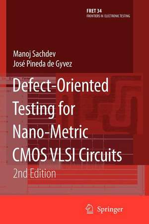
Defect-Oriented Testing for Nano-Metric CMOS VLSI Circuits: Frontiers in Electronic Testing, cartea 34
Autor Manoj Sachdev, José Pineda de Gyvezen Limba Engleză Paperback – 10 noi 2010
| Toate formatele și edițiile | Preț | Express |
|---|---|---|
| Paperback (1) | 1219.46 lei 6-8 săpt. | |
| Springer Us – 10 noi 2010 | 1219.46 lei 6-8 săpt. | |
| Hardback (1) | 1227.36 lei 6-8 săpt. | |
| Springer Us – 21 iun 2007 | 1227.36 lei 6-8 săpt. |
Din seria Frontiers in Electronic Testing
- 15%
 Preț: 639.25 lei
 - 18%
 Preț: 1110.24 lei
 - 18%
 Preț: 948.47 lei
 - 18%
 Preț: 946.55 lei
 - 18%
 Preț: 952.72 lei
 - 18%
 Preț: 944.82 lei
 - 18%
 Preț: 808.75 lei
 - 18%
 Preț: 945.79 lei
 - 18%
 Preț: 1226.24 lei
 - 15%
 Preț: 644.49 lei
 - 15%
 Preț: 649.87 lei
 - 18%
 Preț: 943.07 lei
 - 15%
 Preț: 642.51 lei
 - 18%
 Preț: 948.61 lei
 - 18%
 Preț: 953.65 lei
 - 15%
 Preț: 645.14 lei
 - 15%
 Preț: 644.30 lei
 - 18%
 Preț: 951.29 lei
 - 20%
 Preț: 990.30 lei
 - 18%
 Preț: 968.03 lei
 - 18%
 Preț: 947.35 lei
 - 15%
 Preț: 642.51 lei
 - 15%
 Preț: 646.11 lei
 - 15%
 Preț: 641.85 lei
 - 18%
 Preț: 950.96 lei
Preț: 1219.46 lei
Preț vechi: 1487.15 lei
-18% Nou
Puncte Express: 1829
Preț estimativ în valută:
233.37€ • 242.75$ • 192.66£
233.37€ • 242.75$ • 192.66£
Carte tipărită la comandă
Livrare economică 14-28 aprilie
Preluare comenzi: 021 569.72.76
Specificații
ISBN-13: 9781441942852
ISBN-10: 1441942858
Pagini: 352
Ilustrații: XXI, 328 p.
Dimensiuni: 155 x 235 x 18 mm
Greutate: 0.49 kg
Ediția:Softcover reprint of hardcover 2nd ed. 2007
Editura: Springer Us
Colecția Springer
Seria Frontiers in Electronic Testing
Locul publicării:New York, NY, United States
ISBN-10: 1441942858
Pagini: 352
Ilustrații: XXI, 328 p.
Dimensiuni: 155 x 235 x 18 mm
Greutate: 0.49 kg
Ediția:Softcover reprint of hardcover 2nd ed. 2007
Editura: Springer Us
Colecția Springer
Seria Frontiers in Electronic Testing
Locul publicării:New York, NY, United States
Public țintă
Professional/practitionerCuprins
Functional and Parametric Defect Models.- Digital CMOS Fault Modeling.- Defects in Logic Circuits and their Test Implications.- Testing Defects and Parametric Variations in RAMs.- Defect-Oriented Analog Testing.- Yield Engineering.- Conclusion.
Textul de pe ultima copertă
Failures of nano-metric technologies owing to defects and shrinking process tolerances give rise to significant challenges for IC testing. As the variation of fundamental parameters such as channel length, threshold voltage, thin oxide thickness and interconnect dimensions goes well beyond acceptable limits, new test methodologies and a deeper insight into the physics of defect-fault mappings are needed. In Defect-Oriented Testing for Nano-Metric CMOS VLSI Circuits state of the art of defect-oriented testing is presented from both a theoretical approach as well as from a practical point of view. Step-by-step handling of defect modeling, defect-oriented testing, yield modeling and its usage in common economics practices enables deeper understanding of concepts.
The progression developed in this book is essential to understand new test methodologies, algorithms and industrial practices. Without the insight into the physics of nano-metric technologies, it would be hardto develop system-level test strategies that yield a high IC fault coverage. Obviously, the work on defect-oriented testing presented in the book is not final, and it is an evolving field with interesting challenges imposed by the ever-changing nature of nano-metric technologies. Test and design practitioners from academia and industry will find that Defect-Oriented Testing for Nano-Metric CMOS VLSI Circuits lays the foundations for further pioneering work.
The progression developed in this book is essential to understand new test methodologies, algorithms and industrial practices. Without the insight into the physics of nano-metric technologies, it would be hardto develop system-level test strategies that yield a high IC fault coverage. Obviously, the work on defect-oriented testing presented in the book is not final, and it is an evolving field with interesting challenges imposed by the ever-changing nature of nano-metric technologies. Test and design practitioners from academia and industry will find that Defect-Oriented Testing for Nano-Metric CMOS VLSI Circuits lays the foundations for further pioneering work.
Caracteristici
Wide coverage of topics in test engineering Unique defect-oriented focus of the materials Introduction to yield engineering common practices


